Building an amplifier from discrete transistors requires careful biasing, multiple stages, and resistor networks that drift with temperature. Get the bias wrong and the output clips or distorts; change the transistor and the whole design shifts. An operational amplifier packages all of that complexity into a single IC with predictable, datasheet-guaranteed behavior. With just two external resistors you set the gain, and the circuit works the same whether you use a 5-cent LM358 or a precision OPA2277. In this lesson you will learn five essential op-amp configurations, from inverting amplifiers to comparators, and build a thermistor signal conditioning circuit that maps a weak, nonlinear sensor voltage to the full 0 to 3.3 V range of a microcontroller ADC. #AnalogElectronics #OpAmps #SignalConditioning
The Ideal Op-Amp
An ideal op-amp has these properties:
Property
Ideal Value
Why It Matters
Open-loop gain
Infinite
Amplifies even the tiniest input difference
Input impedance
Infinite
Draws zero current from the source
Output impedance
Zero
Can drive any load without voltage drop
Bandwidth
Infinite
Works at any frequency
Offset voltage
Zero
Output is exactly zero when inputs are equal
Real op-amps approximate these ideals well enough for most applications. The LM358 (dual op-amp, 2 per package) is an excellent beginner part because it works from a single supply (3V to 32V), has rail-to-rail input on the negative side, and costs very little.
Op-Amp Pins
An op-amp has five essential connections:
Pin
Symbol
Description
Non-inverting input
or IN+
Signal appears non-inverted at output
Inverting input
or IN-
Signal appears inverted at output
Output
OUT
Amplified result
Positive supply
or
Positive power rail
Negative supply
or GND
Negative rail or ground (single supply)
The Two Golden Rules
When an op-amp operates with negative feedback (output connected back to the inverting input through a resistor network), these two rules apply:
No current flows into the inputs. The input impedance is so high that the input current is effectively zero.
The op-amp adjusts its output to make both inputs equal. With negative feedback, .
These two rules let you analyze any op-amp circuit by simple algebra.
Five Essential Configurations
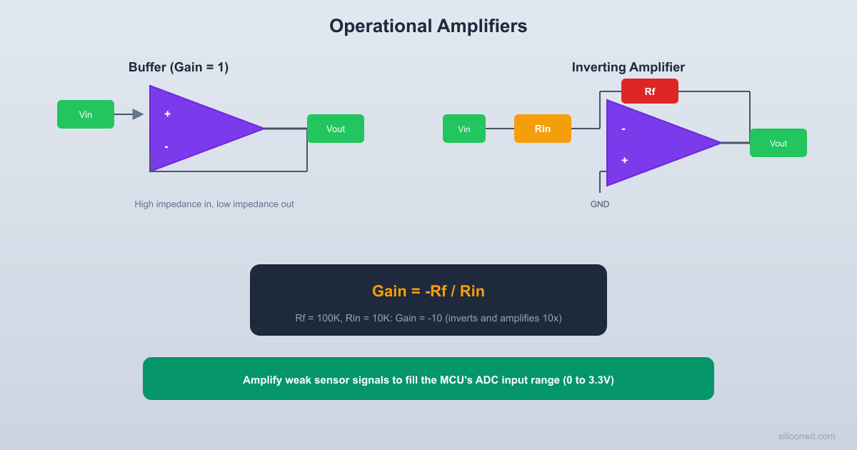
1. Voltage Follower (Buffer)
The simplest op-amp circuit connects the output directly back to the inverting input:
┌──────────┐
V_in ──>─┤ + OUT ├──┬── V_out = V_in
│ │ │
┌──>─┤ - │ │
│ └──────────┘ │
└──────────────────┘
Gain is exactly 1. So why bother? The buffer transforms a high-impedance source (like a voltage divider or sensor) into a low-impedance output that can drive loads without affecting the source voltage.
Embedded application: When you connect a voltage divider to an ADC input, the ADC’s sampling capacitor draws a brief current pulse that disturbs the divider voltage. Placing a buffer between the divider and the ADC eliminates this problem. This is the “source impedance” issue mentioned in STM32 ADC lessons.
2. Non-Inverting Amplifier
The non-inverting amplifier amplifies the input signal without inverting it:
R_f
┌────┤├────┐
│ │
V_in ──>─┤ + OUT ├──┬── V_out
│ │ │
┌──>─┤ - │ │
│ └──────────┘ │
│ │
├──── R_1 ─── GND │
│ │
└──────────────────┘
The gain is always 1 or greater (you cannot attenuate with this configuration). The input impedance is very high, so it does not load the source.
Example: To amplify a sensor signal by a factor of 10, use and :
3. Inverting Amplifier
The inverting amplifier inverts and scales the input:
R_f
┌────┤├────┐
│ │
│ ┌──────┐│
GND ──>─┤ +│ OUT ├┤──── V_out
│ │ │
V_in ──R_in─┤ - │
│ └──────┘
The gain can be less than 1 (attenuation), exactly 1, or greater than 1. The input impedance equals (lower than the non-inverting configuration).
The negative sign means the output is inverted: a positive input produces a negative output. With a single-supply op-amp, the output cannot go below ground (0V), so the inverting amplifier needs a virtual ground or a dual supply to handle negative outputs. For single-supply signal conditioning in embedded systems, the non-inverting configuration is usually preferred.
4. Comparator
When used without feedback (open-loop), an op-amp compares two voltages:
The output snaps to the supply rail or ground, producing a digital output from analog inputs. This is useful for threshold detection: “is the temperature above 50 degrees?” or “is the light level below a threshold?”
  Vcc   |  [R1] 10K            ┌--------┐   +------->  V-  (-)  |        |   |                   |  OUT   +---> Vout  [R2] 10K            |        |  (HIGH or LOW)   |         V+  (+)  |        |  GND   Vsensor -->   └--------┘
  Vref = Vcc x R2/(R1+R2)  Vsensor > Vref: Vout = Vcc  Vsensor < Vref: Vout = 0V
Note: Dedicated comparator ICs (like LM393) are better for this purpose because they have faster response times and open-collector outputs that interface directly with digital logic. But an op-amp works for slow signals and prototyping.
5. Differential Amplifier
A differential amplifier amplifies the difference between two input signals while rejecting signals that are common to both inputs (common-mode rejection):
[R1] [Rf]
V1 o---+--/\/\/--+--+--/\/\/--+
| | |
| V- ┌------┐|
+---->| OUT |+-> Vout
V+ | |
V2 o---+--/\/\/--+--->| |
| [R1] | └------┘
| [Rf]
| |
| GND
|
Vout = (Rf/R1) x (V2 - V1)
This is essential for reading sensors in noisy environments. If electrical noise affects both signal wires equally, the differential amplifier cancels it out. Wheatstone bridges (Lesson 9) produce a differential signal that requires this type of amplifier.
The basic differential amplifier using a single op-amp requires matched resistors for good common-mode rejection. For precision applications, an instrumentation amplifier (three op-amps, or a dedicated IC like the INA128) provides much better performance.
Practical Considerations
Supply Voltage and Output Swing
The LM358 operates from a single supply of 3V to 32V. On a single 5V supply:
The output can swing from about 0V to about 3.5V (not all the way to 5V)
This limits the usable output range for ADC input
Rail-to-rail op-amps (like MCP6002, OPA2340) can swing their output to within millivolts of the supply rails. For 3.3V single-supply systems, rail-to-rail op-amps are strongly recommended.
Bandwidth and Slew Rate
The LM358 has a gain-bandwidth product (GBW) of about 1 MHz. This means:
At gain = 1, bandwidth is 1 MHz
At gain = 10, bandwidth is 100 kHz
At gain = 100, bandwidth is 10 kHz
For audio and low-frequency sensor signals, this is plenty. For high-speed signals, you need a faster op-amp.
Slew rate is how fast the output can change: about 0.3 V/us for the LM358. If you need to amplify a fast signal (like a square wave), the output will round off the edges if the slew rate is insufficient.
Stability and Oscillation
Op-amp circuits can oscillate if the feedback path has too much delay or if the load is capacitive. For most breadboard circuits with resistive feedback, this is not a problem. On PCBs, keep feedback traces short and add a small capacitor (10 to 100 pF) across the feedback resistor if you see oscillation.
Practical Build: Thermistor Signal Conditioning
This is the key project for this lesson. We will read a thermistor voltage, amplify it to fill the 0 to 3.3V range of an ADC, and add a buffer stage for clean readings.
Components Needed
Component
Quantity
Notes
Breadboard
1
From previous lessons
LM358 dual op-amp
1
DIP-8 package
NTC thermistor 10k ohm
1
Standard NTC
Resistors: 1k, 2.2k, 4.7k, 10k, 22k, 47k ohm
2 each
1/4 watt, 1% tolerance preferred
Potentiometer 10k ohm
1
For gain adjustment
Capacitor 100 nF ceramic
2
For power supply decoupling
5V power source
1
USB or regulated supply
Digital multimeter
1
DC voltage mode
Jumper wires
Several
Male-to-male
The Problem
A 10k NTC thermistor in a voltage divider with a 10k fixed resistor produces a voltage that varies from about 0.4V (hot) to 4.6V (cold) on a 5V supply. But the variation over the useful temperature range (say, 20 to 50 degrees Celsius) might only be 1V to 2.5V. If your ADC input range is 0 to 3.3V with 12-bit resolution (4096 counts), using only 1.5V of the 3.3V range wastes half your resolution.
The solution: amplify and offset the signal so that the temperature range of interest fills the entire ADC input range.
Circuit Design
We will use a two-stage approach:
Thermistor Buffer Amplifier
Divider (Op-amp A) (Op-amp B)
┌--------┐ ┌--------┐
VCC--[Rf]--+-->| + OUT |+-->| + OUT |--> Vout
| | | | | (to ADC)
[NTC] | - | | - |
| └---+----┘ └---+----┘
GND | Rf pot |
(output to | |
inv. input) +--[R1]-+
|
GND
Stage 1: Voltage follower (buffer)
The thermistor divider output connects to the non-inverting input of the first LM358 section, with the output connected back to the inverting input. This isolates the thermistor from the amplifier loading.
Stage 2: Non-inverting amplifier
The buffered signal goes to the second LM358 section configured as a non-inverting amplifier with adjustable gain.
Build Steps
Power the LM358
Connect pin 8 () to 5V and pin 4 (GND) to ground. Place a 100 nF ceramic capacitor between pin 8 and pin 4, as close to the IC as possible. This is the decoupling capacitor.
Build the thermistor voltage divider
Connect a 10k fixed resistor from 5V to a node. Connect the 10k NTC thermistor from that node to ground. The voltage at the node varies with temperature.
Connect the buffer (Op-amp A)
Connect the thermistor node to pin 3 (non-inverting input of op-amp A). Connect pin 1 (output A) directly to pin 2 (inverting input A). The output on pin 1 is now a buffered copy of the thermistor voltage.
Build the amplifier (Op-amp B)
Connect pin 1 (buffer output) to pin 5 (non-inverting input of op-amp B). Connect a 10k resistor () from pin 6 (inverting input B) to ground. Connect a 10k potentiometer () from pin 6 to pin 7 (output B).
Set the gain
With the potentiometer at minimum resistance (~0 ohm), gain is about 1. At maximum (10k), gain is . For higher gain, replace with a smaller value. With and (pot) at 10k, gain is .
Measure the output
Use your multimeter to measure the voltage at pin 7 (amplifier output). Warm the thermistor by pinching it between your fingers. The voltage should change noticeably as the thermistor heats up.
Adjust for your ADC range
If your MCU ADC accepts 0 to 3.3V, adjust the gain so the output stays within this range across your expected temperature span. Measure the output at room temperature and while gently warming the thermistor, then set the potentiometer so the maximum output does not exceed 3.3V.
Verify linearity
Note: the thermistor response is not linear. The op-amp amplifies whatever it receives faithfully. Linearization is typically done in software on the MCU using a lookup table or the Steinhart-Hart equation.
LM358 Pinout Reference
Pin
Function
1
Output A
2
Inverting input A
3
Non-inverting input A
4
GND ()
5
Non-inverting input B
6
Inverting input B
7
Output B
8
Verification Checklist
Measurement
Expected Value
Your Measurement
Thermistor divider voltage (room temp, ~25C)
~2.5V
________
Buffer output (pin 1)
Same as divider
________
Amplifier output (gain = 2, room temp)
~5.0V (clipped to ~3.5V by LM358)
________
Amplifier output (gain = 1.5, room temp)
~3.75V
________
Output change when warming thermistor
Decreases (NTC)
________
Supply current (total circuit)
Under 5 mA
________
Dealing with LM358 Output Limitations
You will notice that the LM358 cannot swing its output all the way to 5V. The maximum is typically about . This is actually fine for our purpose, since we want to stay within the 3.3V ADC range. But if you need full rail-to-rail output, consider the MCP6002 (rail-to-rail, works at 3.3V supply) as a drop-in replacement for the LM358 in single-supply circuits.
Common Mistakes
Watch Out For These
No decoupling capacitor on the supply pins: An op-amp without a decoupling capacitor can oscillate at high frequency, producing incorrect output and wasting power. Always add 100 nF ceramic between and GND.
Exceeding input common-mode range: The LM358 inputs can go to ground but not to . If you drive the input above about , the output becomes unpredictable. Check the datasheet for your specific op-amp.
Expecting rail-to-rail from a non-rail-to-rail op-amp: The LM358 output cannot reach . If you need full range, use a rail-to-rail op-amp.
Loading the output: The LM358 can source about 20 mA. Do not try to drive heavy loads (motors, power LEDs) directly from an op-amp output. Use a transistor buffer.
Ignoring gain-bandwidth product: If your gain is 100 and your signal is 50 kHz, the LM358 cannot keep up. Check that .
How This Connects to Embedded Systems
Op-Amps Between Sensors and ADCs
ADC source impedance: Most MCU ADCs require a low-impedance source to charge the internal sampling capacitor quickly. A voltage follower (buffer) solves this. The STM32 reference manual recommends a source impedance below 10k ohm for 12-bit accuracy.
Signal scaling: A sensor that outputs 0 to 200 mV needs to be amplified to 0 to 3.3V for a 12-bit ADC. A non-inverting amplifier with gain of 16.5 does this.
Comparators for threshold detection: An op-amp comparator can generate an interrupt-triggering signal when a sensor crosses a threshold, without any MCU processing overhead.
Active filters: Op-amps combined with resistors and capacitors create active filters (Lesson 7) that provide sharper cutoff characteristics than passive RC filters.
Current sensing: A small shunt resistor in series with a load produces a voltage proportional to current. A differential amplifier reads this voltage while rejecting common-mode noise.
DAC output buffering: If your MCU has a DAC output, buffering it with an op-amp ensures the output voltage remains accurate under load.
Summary
Configuration
Gain Formula
Key Use
Voltage follower
Impedance buffering
Non-inverting
Signal amplification (gain )
Inverting
Amplification with inversion
Comparator
= rail
Threshold detection
Differential
(difference only)
Noise rejection, bridge sensing
Parameter
LM358
MCP6002
Supply range
3 to 32V
1.8 to 6V
Output swing
0 to -1.5V
Rail-to-rail
GBW
1 MHz
1 MHz
Slew rate
0.3 V/us
0.6 V/us
Cost
Very low
Low
Next lesson: power supply design. Every circuit needs clean, stable power. We will build a regulated 3.3V supply from a 9V battery and understand why decoupling matters so much.
Comments