Most real-world signals are analog: temperature, light intensity, pressure, position. The STM32’s 12-bit ADC converts these continuous voltages into discrete numbers your firmware can process. But raw sensor signals are often noisy, weakly driven, or outside the ADC’s input range. This lesson covers the full path from sensor to digital value: voltage dividers, RC filters, op-amp buffers, and the ADC in single, continuous, and DMA scan modes. The project ties it all together into an environmental monitor that reads three analog channels simultaneously. #STM32 #ADC #SignalConditioning
What We Are Building
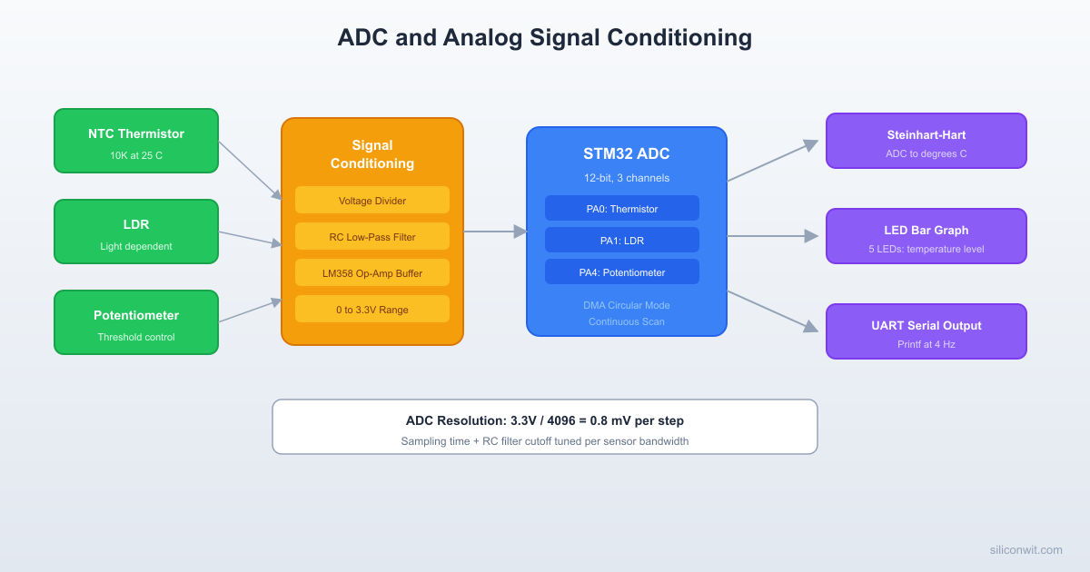
Multi-Channel Environmental Monitor
An environmental monitoring system that reads temperature (NTC thermistor), ambient light (LDR), and a user-adjustable threshold (potentiometer) through three ADC channels. The ADC runs in continuous scan mode with DMA, so the CPU never has to wait for conversions. Temperature is computed using the Steinhart-Hart equation. An LED bar graph (5 LEDs) shows the temperature level visually. The potentiometer sets an alarm threshold: when the temperature exceeds it, the on-board LED blinks. All readings print to a serial terminal over UART2 at 115200 baud.
Project specifications:
Parameter
Value
Board
Blue Pill (STM32F103C8T6, WeAct)
System clock
72 MHz (HSE 8 MHz + PLL x9)
ADC clock
12 MHz (APB2 72 MHz / 6)
ADC resolution
12-bit (0 to 4095)
ADC mode
Continuous scan with DMA circular
Channel 0 (PA0)
Potentiometer (threshold control)
Channel 1 (PA1)
NTC 10K thermistor (voltage divider)
Channel 4 (PA4)
LDR (voltage divider)
LED bar graph
PB0, PB1, PB3, PB4, PB5
Alarm indicator
PC13 (on-board LED, active low)
Serial output
USART2 TX on PA2 (115200 baud)
Update rate
4 Hz on serial terminal
Sampling time
239.5 cycles per channel
Bill of Materials
Component
Quantity
Notes
Blue Pill (STM32F103C8T6)
1
From Lesson 1
ST-Link V2 clone
1
From Lesson 1
NTC 10K thermistor
1
B-value ~3950K
LDR (photoresistor)
1
Resistance varies with light
Potentiometer (10K)
1
Linear taper
LM358 op-amp
1
Dual op-amp, single supply
Resistors (10K)
3
Voltage divider fixed resistors
Resistor (1K)
1
RC filter
Capacitor (100 nF ceramic)
2
RC filter and decoupling
LEDs (5x, any color)
5
Bar graph display
Resistors (330 ohm)
5
LED current limiting
USB-to-serial adapter
1
For UART2 output (or use SWV)
Breadboard + jumper wires
1 set
From Lesson 1
STM32 ADC Architecture
The STM32F103C8T6 has two ADC peripherals (ADC1 and ADC2), each with 12-bit resolution and up to 1 MHz sample rate. For a deeper look at how analog-to-digital converters work internally, including quantization, sampling theory, and DAC counterparts, see Digital Electronics: ADC and DAC Fundamentals. Key parameters you need to understand before configuring the ADC:
Parameter
Value
Why It Matters
Resolution
12 bits
4096 steps from 0 to VDDA
Reference voltage (VDDA)
3.3V
Full scale. 1 LSB = 3.3V / 4096 = 0.806 mV
Input impedance
Varies with sampling time
Short sampling time requires low source impedance
Sampling time
1.5 to 239.5 ADC clock cycles
Longer time allows higher impedance sources
ADC clock
14 MHz maximum
Derived from APB2 with prescaler /2, /4, /6, or /8
Conversion time
Sampling time + 12.5 cycles
At 12 MHz: 239.5 + 12.5 = 252 cycles = 21 us per channel
 Signal Conditioning Pipeline ┌──────────┐  ┌──────────┐  ┌──────────┐  ┌───────┐ │  Sensor  │  │ Voltage  │  │ RC Low-  │  │ STM32 │ │ (NTC,LDR)├─>│ Divider  ├─>│ Pass     ├─>│ ADC   │ │          │  │ 3.3V ref │  │ Filter   │  │ 12-bit│ └──────────┘  └──────────┘  └──────────┘  └───────┘
 Voltage Divider:       RC Filter: 3.3V ─[R_fixed]─┬─     Signal ─[R1 1K]─┬── ADC_IN                  │              [C1 100nF] Sensor ──────────┘                      │                  └─ ADC_IN              GND
Input Impedance and Sampling Time
The ADC input has a sample-and-hold capacitor (about 8 pF internally). During the sampling phase, this capacitor must charge to the input voltage through the source impedance. The datasheet recommends keeping the source impedance below 10K ohm for accurate readings. Longer sampling times allow higher source impedance because the capacitor has more time to settle.
For our sensors, a 239.5-cycle sampling time is generous but ensures accuracy even with the high impedance of the thermistor voltage divider (5K Thevenin equivalent). At 12 MHz ADC clock, each channel takes 21 us, and three channels complete in 63 us. That is fast enough for environmental monitoring.
Single Channel Conversion: Reading the Potentiometer
The simplest ADC usage reads one channel and waits for the result. Connect the potentiometer with its outer pins to 3.3V and GND, and the wiper to PA0.
CubeMX Configuration for Single Channel
Analog > ADC1: enable IN0 (PA0). Set the sampling time to 239.5 cycles.
ADC Settings: keep the default mode (single conversion, no scan, no continuous). This is the simplest starting point.
Generate code and open main.c.
Single channel polling
/* USER CODE BEGIN 2 */
uint32_t adc_raw;
float voltage;
HAL_ADC_Start(&hadc1);
/* USER CODE END 2 */
while (1) {
HAL_ADC_PollForConversion(&hadc1, 10);
adc_raw =HAL_ADC_GetValue(&hadc1);
voltage = (float)adc_raw *3.3f/4095.0f;
HAL_ADC_Start(&hadc1); /* Restart for next conversion */
HAL_Delay(250);
}
This works but blocks the CPU during conversion. For multiple channels, we need scan mode with DMA.
Voltage Divider Sensors
NTC Thermistor
An NTC (Negative Temperature Coefficient) thermistor decreases in resistance as temperature rises. A 10K NTC has 10K ohm at 25 degrees C, about 27K at 0 degrees C, and about 4K at 50 degrees C.
Place the thermistor in a voltage divider with a fixed 10K resistor:
Analog signals pick up noise from nearby digital switching, power supply ripple, and electromagnetic interference. A first-order RC low-pass filter attenuates noise above its cutoff frequency:
For temperature monitoring, the signal changes slowly (seconds). A cutoff frequency of 1.6 kHz (R = 1K, C = 100 nF) removes high-frequency noise while passing the sensor signal through with no visible lag. Place the filter between the voltage divider output and the ADC input pin. For more on filter design and frequency response analysis, see Analog Electronics: Filters and Frequency Response.
Voltage divider output --- [1K] ---+--- PA1 (to ADC)
|
[100 nF]
|
GND
Op-Amp Buffer (LM358 Voltage Follower)
The thermistor voltage divider has a Thevenin output impedance of about 5K ohm (two 10K resistors in parallel). While the long ADC sampling time handles this, a voltage follower guarantees the source impedance is under 100 ohm regardless of the sensor.
The LM358 is a dual op-amp that runs on a single 3.3V supply. Wire one half as a voltage follower:
Voltage divider output ---> (+) LM358
(−) <--- output ---> PA1 (to ADC)
The output follows the input exactly, but can supply milliamps of current to charge the ADC sampling capacitor instantly. The second op-amp in the LM358 package can buffer the LDR channel. For more on op-amp configurations including inverting, non-inverting, and differential amplifiers, see Analog Electronics: Operational Amplifiers.
Rail-to-rail note. The LM358 output cannot swing all the way to the positive rail. On a 3.3V supply, the maximum output is about 2.0 to 2.5V (depends on load). This means your ADC will never see voltages above about 2.5V from the buffered output. For a temperature sensor that operates in the 1.0 to 2.5V range, this is acceptable. If you need full 0 to 3.3V swing, use a rail-to-rail op-amp like the MCP6002 or TLV2372 instead.
Multi-Channel Scan Mode with DMA
Reading three channels one at a time with polling is wasteful. The STM32 ADC supports scan mode, where it converts a sequence of channels automatically. Combined with DMA (Direct Memory Access), the conversion results are transferred to a memory buffer without any CPU intervention.
ADC Continuous Scan + DMA
┌───────────────────────────────┐
│ ADC1 Scan Sequence │
│ CH0──>CH1──>CH4──>CH0──>... │
│ (pot) (NTC) (LDR) repeat │
└──────────┬────────────────────┘
│ DMA1 Channel 1
v (automatic transfer)
┌──────────────────────┐
│ adc_buffer[3] │
│ [0] = pot (PA0) │ CPU reads
│ [1] = temp (PA1) │ buffer at
│ [2] = light(PA4) │ any time
└──────────────────────┘
Circular mode: DMA restarts
after 3 transfers, zero CPU
CubeMX Configuration for DMA Scan Mode
Analog > ADC1: enable IN0 (PA0), IN1 (PA1), and IN4 (PA4). Set sampling time to 239.5 cycles for all three.
ADC1 Parameter Settings: set Scan Conversion Mode to Enabled, Continuous Conversion Mode to Enabled, Number of Conversions to 3. Configure the rank sequence: Rank 1 = Channel 0 (pot), Rank 2 = Channel 1 (thermistor), Rank 3 = Channel 4 (LDR).
DMA Settings tab for ADC1: click Add and select ADC1. Set Mode to Circular, Data Width to Half Word (16-bit), and enable Memory increment. Circular mode means DMA restarts from the beginning of the buffer automatically.
Connectivity > USART2: enable in Asynchronous mode, 115200 baud, 8N1. This uses PA2 (TX) and PA3 (RX).
GPIO Outputs: configure PB0, PB1, PB3, PB4, PB5 as GPIO_Output for the LED bar graph. Configure PC13 as GPIO_Output for the alarm LED.
Generate code.
DMA Buffer
DMA needs a memory buffer that it writes to continuously. Declare it as a global array:
In the project settings, enable “Use float with printf” under C/C++ Build > Settings > MCU Settings so that %f format works with floating point values.
Wiring Diagram
Blue Pill Pin
Connection
Notes
PA0
Potentiometer wiper
Outer pins to 3.3V and GND
PA1
Thermistor voltage divider output
Through RC filter (1K + 100nF) to pin
PA2
USART2 TX
To USB-serial adapter RX
PA3
USART2 RX
To USB-serial adapter TX
PA4
LDR voltage divider output
Through RC filter if desired
PB0
LED bar 1 (lowest)
Through 330 ohm to GND
PB1
LED bar 2
Through 330 ohm to GND
PB3
LED bar 3
Through 330 ohm to GND
PB4
LED bar 4
Through 330 ohm to GND
PB5
LED bar 5 (highest)
Through 330 ohm to GND
PC13
On-board LED
Active low, alarm indicator
3.3V
Sensor dividers, pot, LM358 VCC
Common 3.3V rail
GND
Common ground
All GNDs connected
PA13
ST-Link SWDIO
Debug interface
PA14
ST-Link SWCLK
Debug interface
LM358 wiring (optional buffer):
LM358 Pin
Connection
Notes
Pin 8 (VCC)
3.3V
Single supply
Pin 4 (GND)
GND
Pin 3 (IN1+)
Thermistor divider output
Before RC filter
Pin 2 (IN1−)
Pin 1 (OUT1)
Feedback for voltage follower
Pin 1 (OUT1)
PA1 through RC filter
Buffered thermistor signal
Pin 5 (IN2+)
LDR divider output
Pin 6 (IN2−)
Pin 7 (OUT2)
Feedback for voltage follower
Pin 7 (OUT2)
PA4
Buffered LDR signal
Complete Project Code
main.c
/* USER CODE BEGIN Header */
/**
* Environmental Monitor - ADC and Analog Signal Conditioning
* Sensor and Actuator Interfacing with STM32, Lesson 2
*
* Reads thermistor, LDR, and potentiometer via ADC with DMA.
* Displays temperature on LED bar graph and prints to UART.
*/
/* USER CODE END Header */
/* Includes ------------------------------------------------------------------*/
ADC calibration runs once at startup. The STM32F1 ADC has a built-in self-calibration routine that compensates for internal offset errors. Always call this before the first conversion.
HAL_ADC_Start_DMA launches the ADC in continuous scan mode. DMA transfers each conversion result into adc_dma_buf[0..2] in the order defined by the scan sequence (Rank 1, 2, 3). In circular mode, DMA wraps back to index 0 after the last channel, so the buffer always contains the most recent readings.
ADC_To_Temperature converts the raw ADC value to thermistor resistance using the voltage divider formula, then applies the Beta equation to get temperature in degrees Celsius. The function returns -999 if the ADC value is at the rail (sensor disconnected).
UpdateLedBarGraph maps the temperature to a 0 to 5 level and lights the corresponding LEDs. At 15 degrees C all LEDs are off; at 40 degrees C all five are lit.
CheckAlarmThreshold maps the potentiometer voltage to a temperature threshold in the same 15 to 40 degrees C range. When the measured temperature exceeds the threshold, the on-board LED (PC13) blinks. Turning the pot clockwise raises the threshold.
The main loop reads the DMA buffer, converts values, updates outputs, and prints to the serial terminal at 4 Hz. The DMA runs independently, so the main loop never waits for ADC conversions.
Steinhart-Hart vs. Beta Equation
The full Steinhart-Hart equation uses three coefficients (A, B, C) and is accurate across a wide temperature range. The simplified Beta equation uses only one coefficient and is accurate within about 1 degree C over a 50-degree window centered on 25 degrees C. For environmental monitoring (indoor temperatures from 10 to 45 degrees C), the Beta equation is sufficient.
If you need higher accuracy, use the full Steinhart-Hart coefficients from your thermistor datasheet:
Full Steinhart-Hart (reference)
/* Example coefficients for a Murata NCP18XH103F03RB */
ADC grounding. The STM32F103 has separate VDDA and VSSA pins for the analog supply. On a PCB, connect VDDA to 3.3V through a ferrite bead (e.g., BLM18PG121SN1) and place a 1 uF + 100 nF capacitor pair as close to VDDA as possible. Never route digital signals under the ADC input traces.
Star ground topology. Run separate ground traces from the analog sensors and from the digital outputs (LEDs, relay) back to a single point near the STM32 GND pin. This prevents switching current from the LEDs from injecting noise into the analog ground.
Decoupling capacitors. Place a 100 nF ceramic capacitor within 5 mm of every IC power pin. The LM358, the STM32 VDD pins, and any sensor module VCC each need their own decoupling cap. Use 0402 or 0603 size for short trace lengths.
Guard traces. For high-impedance analog inputs (like the thermistor divider), surround the PCB trace with a guard ring connected to the op-amp output or to analog ground. This prevents leakage currents from adjacent traces from corrupting the measurement. A 1 nA leakage across a 10K impedance causes a 10 uV error, which is below 1 LSB, but it adds up in humid environments.
Thermal considerations. Mount the NTC thermistor away from heat-generating components (voltage regulators, power resistors). On a PCB, the copper pour acts as a heat sink that can bias the temperature reading. Use a thermal relief pattern or mount the thermistor on a small breakout with minimal copper.
Comments