Place a ground pour trace under the ESP32’s antenna and your WiFi range drops from 30 meters to 3. Route a high-speed signal through the antenna keepout zone and the module may fail to connect at all. Wireless PCB design has rules that do not exist for purely digital boards, and violating them produces failures that look like firmware bugs because the code is correct but the radio cannot hear the access point. In this lesson you will design an ESP32-WROOM-32 development board with a CP2102N USB-UART bridge and auto-reset circuit, then lay out a 2-layer PCB that respects the antenna keepout zone and maintains ground plane continuity for reliable wireless performance. #KiCad #ESP32 #RFDesign
Antenna Keepout Zone (top view)
──────────────────────────────────────────
┌──────────────────────────────────────┐
│ ┌─────────┐ │
│ Components OK here │ ESP32 │ │
│ (USB, LDO, caps, etc.) │ WROOM │ │
│ │ │ │
│ │ ┌─────┐ │ │
│ │ │Ante-│ │ │
│ NO copper, │ │nna │ │ │
│ NO traces, │ └─────┘ │ │
│ NO components ──┼─►KEEPOUT│ │
│ in this zone └─────────┘ │
│ ◄── 15mm ──►│
└──────────────────────────────────────┘
Board edge must not obstruct antenna.
What We Are Building
ESP32 WiFi/Bluetooth Development Kit
A DevKitC-style development board built around the ESP32-WROOM-32 module. The board features a CP2102N USB-UART bridge for programming and serial communication, an auto-reset circuit that puts the ESP32 into bootloader mode automatically, and dual 19-pin headers exposing all GPIO. Power comes from USB Micro-B through an AMS1117-3.3 LDO.
Board specifications:
Parameter
Value
Module
ESP32-WROOM-32 (integrated antenna, 4 MB flash)
USB-UART
CP2102N (internal oscillator, no external crystal)
USB
Micro-B for power and programming
Power
AMS1117-3.3 LDO, 5V USB input
Auto-reset
RTS/DTR to EN/GPIO0 via NPN transistors
Buttons
EN (reset) and BOOT (GPIO0)
User LED
GPIO2 with 330 ohm resistor
Headers
2x 19-pin, 2.54mm pitch (all GPIO)
Board size
~55 x 28 mm
Bill of Materials
Ref
Component
Package
Qty
Notes
U1
ESP32-WROOM-32
Module (18x25.5mm)
1
Integrated antenna and shielding
U2
CP2102N-A02-GQFN28
QFN-28 (5x5mm)
1
USB-UART bridge, internal oscillator
U3
AMS1117-3.3
SOT-223
1
3.3V 1A LDO
J1
USB Micro-B
SMD
1
Power and data
J2, J3
1x19 pin header
2.54mm
2
GPIO breakout
Q1, Q2
S8050 (or 2N7002)
SOT-23
2
Auto-reset transistors
  Auto-Reset Circuit  ──────────────────────────────────────────  CP2102N                  ESP32  ─────────                ─────  DTR ──► Q1 (NPN) ─────► GPIO0 (BOOT)          │  RTS ──► Q2 (NPN) ─────► EN (RESET)
  Programming sequence:  1. DTR=LOW, RTS=HIGH → EN=LOW (reset)  2. DTR=HIGH, RTS=LOW → GPIO0=LOW (boot)  3. DTR=HIGH, RTS=HIGH → EN=HIGH (run)  ESP32 enters bootloader automatically.  No manual button presses needed.
Reference
Value
Package
Qty
Function
C1, C2
10 µF
0805
2
LDO input/output
C3, C4
100 nF
0402
2
ESP32 VDD decoupling
C5
100 nF
0402
1
CP2102N decoupling
C6
100 nF
0402
1
EN pin RC filter
C7
4.7 µF
0805
1
USB VBUS decoupling
R1
10 kΩ
0402
1
EN pull-up
R2
10 kΩ
0402
1
GPIO0 pull-up
R3, R4
10 kΩ
0402
2
Auto-reset base/gate resistors
R5
330 Ω
0402
1
User LED
D1
Blue LED
0402
1
User LED (GPIO2)
SW1
Tactile switch
SMD 3x6mm
1
EN (reset)
SW2
Tactile switch
SMD 3x6mm
1
BOOT (GPIO0)
F1
500 mA polyfuse
0805
1
VBUS protection
ESP32 Module Overview
The ESP32-WROOM-32 is a module, not a bare chip. Inside the metal shielding can, Espressif has already placed the ESP32 SoC, a 40 MHz crystal, 4 MB SPI flash, and all the required passives. The PCB antenna is etched onto the module’s own PCB and extends beyond the metal can at one end. This is the part you need to keep clear of copper on your board.
Using a module instead of the bare ESP32 SoC saves you significant design effort. The RF matching network between the SoC and the antenna is already tuned and tested. The module carries FCC, CE, and other wireless certifications, which means your product can reference the module’s certification rather than going through the full (and expensive) RF certification process from scratch.
Key Pins
Pin
Function
Notes
EN
Chip enable
Active high, must have RC filter (10 kΩ + 100 nF)
GPIO0
Boot mode strapping
LOW at reset = bootloader, HIGH = normal boot
TXD0 (GPIO1)
UART0 TX
Default serial output, connects to CP2102N RXD
RXD0 (GPIO3)
UART0 RX
Default serial input, connects to CP2102N TXD
GPIO2
Strapping pin
Must be LOW or floating during boot. Safe for LED after boot
VDD 3.3V
Power supply
Multiple pins, all must be connected
GND
Ground
Multiple pins, all must be connected
Strapping Pins
The ESP32 samples several GPIO pins at reset to determine boot mode and other configuration. The critical ones for this board:
Pin
Boot from Flash
Boot to Bootloader
GPIO0
HIGH (default pull-up)
LOW (held by BOOT button or auto-reset)
GPIO2
LOW or floating
LOW or floating
Do not connect heavy loads to GPIO0, GPIO2, GPIO5, GPIO12, or GPIO15 without understanding their strapping behavior. The ESP32 datasheet and the WROOM-32 module datasheet both document these requirements.
RF-Aware Design Principles
This is what separates an ESP32 board that works reliably from one that drops WiFi connections or has poor range. The layout around the antenna area directly affects wireless performance.
Antenna keepout zone. The WROOM-32 module has a PCB antenna that extends beyond the edge of the metal shielding can. No copper of any kind (no traces, no ground pour, no component pads) should exist underneath or within 2mm around the antenna section of the module. This means no copper on any layer in that region. Copper near the antenna detunes it, shifting its resonant frequency away from the 2.4 GHz band and reducing both transmit power and receive sensitivity.
Ground plane continuity. While you must keep copper away from the antenna, you need a solid, unbroken ground plane under the rest of the module body (the shielded section). The ESP32’s ground pins connect to this plane, and the RF return currents flow through it. Splits or gaps in the ground plane under the module degrade performance just as much as copper under the antenna.
Decoupling near power pins. Place 100 nF capacitors as close as possible to the module’s VDD pins. The ESP32 draws current in sharp bursts during WiFi transmission (peaks over 300 mA), and poor decoupling causes voltage droops that can crash the module or corrupt transmitted packets.
Keep digital signals away from the antenna. Route all traces on the opposite side of the module from the antenna. High-speed switching signals (SPI clock, I2C, PWM) radiate noise that can interfere with the 2.4 GHz band if they run near the antenna area.
Antenna Keepout Summary
Zone
Copper Allowed?
Components Allowed?
Under antenna (beyond metal can)
No, on any layer
No
Within 2mm of antenna edges
No, on any layer
No
Under metal shielding can
Yes, ground plane required
Decoupling caps on back side OK
Board edge near antenna
Board must extend to module edge or beyond
No connectors near antenna end
Schematic Capture
Create a new KiCad project named esp32-devkit. Open the schematic editor and build the following sub-circuits.
Place the USB Micro-B connector. Add USB_B_Micro from the Connector library. This provides VBUS (5V), D+, D-, ID, and GND.
Add VBUS protection. Connect VBUS through polyfuse F1 (500 mA) to a net labeled VBUS_5V. Place a 4.7 µF decoupling capacitor (C7) from VBUS_5V to GND near the connector.
Place the AMS1117-3.3 LDO (SOT-223). Connect VBUS_5V to the input pin through a 10 µF capacitor (C1). Connect the output to a +3V3 power net through a 10 µF capacitor (C2). The AMS1117 also needs the input cap for stability.
Add power flags. Place PWR_FLAG symbols on +3V3 and GND if ERC reports undriven power nets.
ESP32-WROOM-32 Module
Place the ESP32 module. Add ESP32-WROOM-32 from the RF_Module library. The symbol shows all exposed pins of the module including the ground pad.
Connect all power pins. Wire every VDD pin to +3V3 and every GND pin (including the large ground pad) to GND. The WROOM-32 has multiple ground pins; all must be connected for proper RF return currents.
EN pin circuit. Connect EN to +3V3 through a 10 kΩ pull-up resistor (R1). Place a 100 nF capacitor (C6) from EN to GND. This RC filter prevents noise from accidentally resetting the module. The EN pin also connects to the auto-reset circuit and the EN pushbutton (SW1).
GPIO0 strapping. Connect GPIO0 to +3V3 through a 10 kΩ pull-up resistor (R2). This ensures normal boot from flash. GPIO0 also connects to the auto-reset circuit and the BOOT pushbutton (SW2).
UART0 connections. Connect TXD0 (GPIO1) to the CP2102N RXD pin. Connect RXD0 (GPIO3) to the CP2102N TXD pin. Note the crossover: the ESP32 TX goes to the bridge RX, and vice versa.
Decoupling capacitors. Place 100 nF caps (C3, C4) on the VDD pins, as close to the module as possible in the schematic. Physical placement matters more, but schematic proximity helps during layout.
User LED. Connect GPIO2 through a 330 ohm resistor (R5) to the anode of D1 (blue LED), cathode to GND. GPIO2 is safe to use as a user LED after boot completes.
GPIO headers. Place two 1x19 pin headers (J2, J3) and route all remaining GPIO pins to them. Follow the ESP32-DevKitC pinout order if you want compatibility with existing tutorials and shields.
CP2102N USB-UART Bridge
Place the CP2102N. Add CP2102N-A02-GQFN28 from the Interface_USB library (or create a custom symbol if not available). The CP2102N has an internal oscillator, so you do not need an external 12 MHz crystal. This simplifies the design compared to the older CP2102.
USB data lines. Connect the USB Micro-B D+ and D- pins to the CP2102N’s D+ and D- pins. The CP2102N handles all USB protocol internally.
Power connections. Connect the CP2102N VDD pin to +3V3 and VBUS to the VBUS pin (if available on the package) or to +3V3 through the regulator. Add a 100 nF decoupling capacitor (C5) from VDD to GND.
UART pins. Connect CP2102N TXD to ESP32 RXD0 (GPIO3). Connect CP2102N RXD to ESP32 TXD0 (GPIO1).
Control signals. Bring out the RTS and DTR pins. These connect to the auto-reset circuit described next. The CP2102N asserts these signals when the programming tool (esptool or Arduino IDE) requests a reset into bootloader mode.
Auto-Reset Circuit
This is the circuit that makes one-click programming possible. Without it, you would need to hold the BOOT button, press EN, release BOOT, and then click upload every time you flash new firmware.
The auto-reset circuit uses two NPN transistors (or N-channel MOSFETs) to translate the CP2102N’s DTR and RTS signals into the correct sequence on EN and GPIO0. When the programming tool begins an upload, it asserts DTR low and pulses RTS. The transistor cross-coupling converts this into: first pull GPIO0 low (enter bootloader mode), then pulse EN low (reset the chip). The ESP32 resets, samples GPIO0 low, and enters the bootloader. The programming tool then uploads the firmware over UART.
Transistor Q1 (controls EN). Connect the collector to the EN net. Connect the emitter to GND. Connect the base through a 10 kΩ resistor (R3) to the RTS signal from CP2102N.
Transistor Q2 (controls GPIO0). Connect the collector to the GPIO0 net. Connect the emitter to GND. Connect the base through a 10 kΩ resistor (R4) to the DTR signal from CP2102N.
Cross-coupling. Add a 100 nF capacitor from DTR to the EN net (in parallel with Q1’s path). Add a 100 nF capacitor from RTS to the GPIO0 net (in parallel with Q2’s path). This capacitor coupling ensures the correct timing sequence. The exact topology follows the ESP32-DevKitC reference design published by Espressif.
Manual buttons. Wire SW1 (EN button) between the EN net and GND. Wire SW2 (BOOT button) between GPIO0 and GND. These allow manual reset and bootloader entry when no USB is connected.
ERC and Footprint Assignment
Run ERC. Click Inspect > Electrical Rules Checker. Common warnings to address: unconnected GPIO pins (add “no connect” flags if intentionally unused), missing power flags, and conflicting pin types on the USB data lines.
Assign footprints. Open Tools > Assign Footprints. Key assignments:
ESP32-WROOM-32: RF_Module:ESP32-WROOM-32 (the official KiCad footprint includes the antenna keepout courtyard)
Generate the netlist. Click Tools > Update PCB from Schematic (or press F8) to transfer the schematic to the PCB editor.
PCB Layout
Board Outline and Module Placement
Draw the board outline. Switch to the Edge.Cuts layer and draw a rectangle approximately 55mm x 28mm. The ESP32 module is 18mm wide, so 28mm gives adequate clearance on both sides for pin headers.
Place the ESP32 module at one short edge. Position the module so the antenna section extends to (or slightly beyond) the board edge. The antenna must point outward with no board material or components blocking it. Align the module center with the board center horizontally.
Place the USB connector at the opposite short edge. This maximizes the distance between the USB connector (a source of digital noise) and the antenna. The USB connector’s metal shell should align flush with the board edge.
Place the LDO between USB and ESP32. Position the AMS1117-3.3 and its capacitors along the power path from USB to the module. Keep the power traces short and direct.
Place the CP2102N near the USB connector. The USB data lines should be as short as possible between the connector and the UART bridge. Place C5 (decoupling) adjacent to the CP2102N VDD pin.
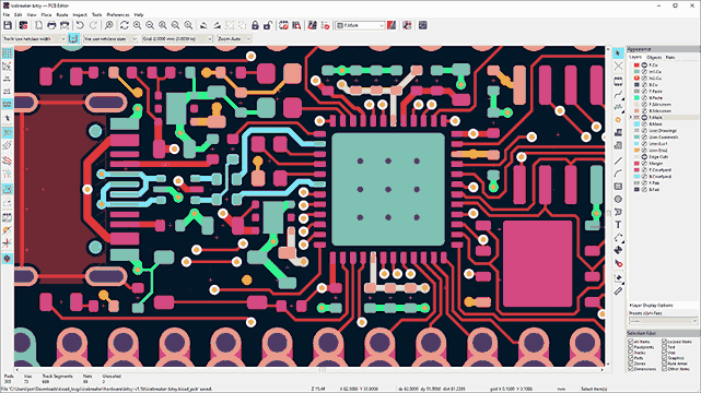
Antenna Keepout Zone in KiCad
Identify the antenna area. The ESP32-WROOM-32 footprint in KiCad includes a courtyard that marks the antenna region. The antenna extends approximately 5mm beyond the metal shielding can at the top of the module.
Draw a Rule Area. Select Add Rule Area (also called Keep Out Zone) from the right toolbar. In the properties dialog, check “Keep out copper pour” for all copper layers (F.Cu, B.Cu). Draw a rectangle covering the entire antenna area plus 2mm margin on all sides.
Verify no copper exists in the keepout. After filling zones (press B), visually inspect the antenna area. There should be no ground pour, no traces, and no vias within the keepout rectangle on any copper layer.
Board edge alignment. If the antenna extends beyond the board edge, the Edge.Cuts outline should follow the module edge at the antenna end. Some designers extend the board slightly beyond the antenna for mechanical protection, but leave the extended area completely free of copper.
Ground Pour and Plane Strategy
This is a 2-layer board, so you do not have dedicated inner planes. Instead, use copper pours on both F.Cu and B.Cu assigned to GND. The key rule: the ground pour must be solid and unbroken under the shielded body of the ESP32 module, but completely absent under the antenna area.
On F.Cu, the ground pour fills around the component pads and traces. On B.Cu, the pour should be as continuous as possible, especially under the ESP32 module. Connect the front and back ground pours with via stitching every 3 to 5mm. This creates a pseudo-ground-plane that improves RF performance on a 2-layer board.
Create GND zone on F.Cu. Add a filled zone covering the entire board, assigned to the GND net. Set zone priority to 0.
Create GND zone on B.Cu. Same process on B.Cu, also assigned to GND with priority 0.
Add via stitching. Place GND vias every 3 to 5mm across the board area (except in the antenna keepout zone). Concentrate stitching vias around the ESP32 module’s ground pad area and along the board edges.
Verify ground continuity. After filling zones, use the net inspector to confirm that all GND pads are connected to the same net. Look for isolated ground islands caused by trace routing that could split the pour.
Component Placement Summary
Priority
Component
Placement Rule
1
ESP32-WROOM-32
Board edge, antenna pointing outward
2
USB Micro-B
Opposite board edge from antenna
3
CP2102N
Near USB connector, short D+/D- traces
4
AMS1117-3.3 + caps
Between USB and ESP32, short power path
5
Auto-reset transistors
Near CP2102N and ESP32 EN/GPIO0 pins
6
Decoupling caps (C3, C4)
Adjacent to ESP32 VDD pins, back side OK
7
Buttons (EN, BOOT)
Board edge for easy access
8
GPIO headers
Both long edges of the board
Trace Routing Tips
Route the USB D+ and D- traces first, keeping them short and parallel between the Micro-B connector and the CP2102N. These are USB 2.0 Full-Speed (12 Mbps) signals, so keep them under 50mm total length and avoid sharp 90-degree bends.
Route the UART lines (TXD, RXD) between the CP2102N and the ESP32 module next. These run at up to 921600 baud during programming, which is slow enough that trace impedance is not critical. Keep them away from the antenna area.
Route power traces (VBUS to LDO input, LDO output to 3V3 net) with wider traces (0.5mm or more) to handle the ESP32’s peak current draw during WiFi transmission (up to 500 mA from the 3.3V rail).
Route all remaining GPIO connections to the pin headers last. Keep traces away from the antenna end of the board.
Design Rules for JLCPCB 2-Layer
Set these minimum design rules in Board Setup > Design Rules > Constraints:
Parameter
Minimum
Recommended
Trace width
0.127 mm
0.25 mm (0.5 mm for power)
Trace spacing
0.127 mm
0.2 mm
Via drill
0.3 mm
0.3 mm
Via diameter
0.6 mm
0.6 mm
Copper to edge
0.2 mm
0.3 mm
Running DRC
Fill all zones (Edit > Fill All Zones, or press B).
Open Inspect > Design Rules Checker.
Fix any clearance violations, unconnected nets, or minimum width violations.
Pay special attention to the antenna keepout zone. Verify that DRC does not report any copper inside the keepout area.
Manufacturing
The Gerber and drill file export process is the same as Lesson 3. Generate Gerbers for F.Cu, B.Cu, F.Mask, B.Mask, F.SilkS, B.SilkS, and Edge.Cuts, plus the drill file. Zip everything and upload to JLCPCB.
For a 2-layer board this size (55x28mm), expect to pay 5 for 5 boards at JLCPCB. Select 1.6mm board thickness and HASL surface finish. If you plan to hand-solder the QFN-28 CP2102N, consider ENIG finish for flatter pads, though HASL works fine with careful technique. The ESP32 module itself is castellated (half-vias on the edges) and can be soldered with a standard iron by applying flux and tacking each pad.
For a full walkthrough of the JLCPCB ordering process including BOM and pick-and-place file generation, refer back to Lesson 3.
Firmware: WiFi Scan
Once the board is assembled, verify that the ESP32 boots correctly and WiFi works by running a network scan. We use the Arduino framework for simplicity, since it handles all the ESP-IDF configuration behind the scenes.
Arduino IDE Setup
Install ESP32 board support. In Arduino IDE, go to File > Preferences and add https://espressif.github.io/arduino-esp32/package_esp32_index.json to the Additional Board Manager URLs. Then open Tools > Board > Boards Manager, search for “esp32”, and install the Espressif package.
Select the board. Go to Tools > Board > ESP32 Arduino and select “ESP32 Dev Module”.
Select the port. Plug in the board via USB. The CP2102N should enumerate as a serial port. On Linux it appears as /dev/ttyUSB0, on Windows as a COM port, and on macOS as /dev/tty.usbserial-XXXX. Select it under Tools > Port.
Set upload speed. Under Tools > Upload Speed, select 921600 for fast programming. The auto-reset circuit handles the bootloader entry automatically.
WiFi Scan Sketch
/*
* ESP32 WiFi Scanner
* Scans for nearby WiFi networks and prints results over serial.
* Upload via USB with auto-reset (just click Upload in Arduino IDE).
If the board does not respond after clicking Upload:
Check the auto-reset circuit. Hold the BOOT button, press and release EN, then release BOOT. Click Upload again. If this works but auto-reset does not, inspect the transistor wiring and the DTR/RTS connections from the CP2102N.
Verify 3.3V power. Measure the voltage on the ESP32 VDD pins. It should be 3.3V plus or minus 0.1V. Low voltage (below 3.0V) indicates an LDO or capacitor problem.
Check serial port. If no serial port appears when you plug in the board, the CP2102N may not be soldered properly. Check for solder bridges on the QFN pads, especially between adjacent pins.
WiFi scan returns zero networks. Check the antenna keepout zone on your PCB. Copper under the antenna is the most common cause of poor WiFi performance on custom ESP32 boards. Also verify that no metal enclosure or your hand is covering the antenna during testing.
What You Have Learned
Lesson 5 Complete
KiCad skills:
Designed an RF-aware PCB layout with antenna keepout zones using Rule Areas
Managed ground pour continuity on a 2-layer board for wireless module performance
Placed components to maximize antenna clearance and minimize noise coupling
Applied via stitching for ground plane integrity on a 2-layer wireless board
Comments