Through-hole components are easy to solder, but they are large, limit how dense your layout can be, and many modern sensors simply do not come in through-hole packages. If you want to use the latest MEMS sensors, IMUs, or compact MCU variants, you need to work with SMD. Surface mount parts can be ten times smaller, which means shorter traces, less parasitic capacitance, and boards that fit in tight enclosures. In this lesson you will design a sensor shield around the ATmega328P in a TQFP-32 package, add an I2C temperature/humidity sensor (SHT30) and an SPI ambient light sensor (VEML7700), and learn CNC milling as an alternative to chemical etching. #KiCad #SMD #SensorShield
  SMD Component Size Comparison  ──────────────────────────────────────────  Through-hole resistor (axial):  ├────────── 6.5 mm ──────────┤
  0805 SMD (2.0 x 1.25 mm):  ├──┤  ◄── fits on a pencil tip
  0402 SMD (1.0 x 0.5 mm):  ├┤    ◄── barely visible
  TQFP-32 (0.8mm pitch):  ┌──────────┐  │ ││││││││ │  32 pins total,  │          │  8 per side,  │ ││││││││ │  0.8 mm between  └──────────┘  pin centers
What We Are Building
ATmega328P Sensor Shield
A compact double-sided sensor board with the ATmega328P in its smallest through-hole-free package (TQFP-32, 0.8mm pin pitch). The board reads temperature, humidity, and ambient light through I2C and SPI buses, sending data over UART. All passives are 0805 SMD, the smallest size comfortable for hand soldering.
Board specifications:
Parameter
Value
MCU
ATmega328P-AU (TQFP-32, 0.8mm pitch)
Clock
16 MHz crystal (3.2x2.5mm SMD)
Power
USB Micro-B 5V input, 3.3V LDO (AMS1117-3.3) for sensors
Before drawing the schematic, let’s understand what changes with SMD components.
Package Sizes
SMD passive components come in standardized sizes named by their imperial dimensions in hundredths of an inch:
Package
Size (mm)
Hand Solderable?
Use Case
1206
3.2 x 1.6
Easy
Prototypes, power resistors
0805
2.0 x 1.25
Comfortable
General purpose (this lesson)
0603
1.6 x 0.8
Moderate
Space-constrained designs
0402
1.0 x 0.5
Difficult
Professional assembly only
We use 0805 throughout this lesson. It is small enough to save board space but large enough that a steady hand with a fine-tip soldering iron can handle it.
TQFP vs DIP
The ATmega328P-AU (TQFP-32) has the same silicon as the DIP-28 version from Lesson 1, but in a 7x7mm package instead of 37x7mm. The pin pitch drops from 2.54mm to 0.8mm. This means:
Thinner traces between pins (you need at least 0.2mm trace width to route between TQFP pads)
Solder paste and a hot air station work better than an iron for TQFP soldering
The pinout maps differently: TQFP-32 has 32 pins (4 extra: two additional GND and two ADC pins)
Pad and Courtyard
In KiCad, every SMD footprint has:
Pads: copper areas where solder connects the component to the board
Courtyard: a clearance boundary showing how close other components can be placed
Fab layer: the component outline showing its physical dimensions
When placing components, keep courtyards from overlapping. KiCad’s DRC checks this automatically.
Schematic Capture
Create a new KiCad project named atmega328p-sensor-shield.
This board has two voltage rails: 5V from USB for the MCU, and 3.3V from the LDO for the sensors.
Place the USB Micro-B connector. Add USB_B_Micro from the Connector library. This provides 5V and GND from any USB power source.
Place the 3.3V LDO. Add AMS1117-3.3 (SOT-223). Connect its input to the USB 5V through a 10 µF capacitor (C7). Connect its output to a +3V3 power symbol through another 10 µF capacitor (C8).
Add power symbols. Place +5V, +3V3, and GND power symbols. The MCU runs on +5V; the sensors run on +3V3.
Wire the power section. USB VBUS to +5V, USB GND to GND. LDO input from +5V, LDO output to +3V3.
MCU and Crystal
Place the ATmega328P-AU. Add ATmega328P-AU (the TQFP-32 variant). Place it in the center of the schematic.
Connect power. Wire VCC (pin 4), AVCC (pin 18) to +5V. Wire GND (pins 3, 5, 21) to GND. Place 100 nF decoupling capacitors (C3, C4) close to VCC and AVCC.
Crystal circuit. Place a Crystal_SMD_4Pin (16 MHz) between XTAL1 (pin 7) and XTAL2 (pin 8). Add 22 pF load capacitors (C1, C2) from each crystal pin to GND.
Reset circuit. Connect a 10 kΩ pull-up (R1) from RESET (pin 29) to +5V. Add the SMD tactile switch from RESET to GND.
ISP header. Place Conn_AVR_ISP and wire MISO, MOSI, SCK, RESET, VCC, GND as in Lesson 1.
I2C Bus and Sensors
Both the SHT30 and VEML7700 communicate over I2C, so they share the same bus.
I2C pull-ups. Add two 4.7 kΩ resistors (R2, R3). Connect R2 from SDA (PC4/pin 27) to +3V3. Connect R3 from SCL (PC5/pin 28) to +3V3. We pull up to 3.3V because both sensors are 3.3V devices. The ATmega328P I2C pins are 3.3V tolerant when running at 5V.
Place the SHT30. Add SHT3x-DIS (or create a custom symbol with VDD, GND, SDA, SCL, ADDR, ALERT pins). Connect VDD to +3V3, GND to GND, SDA to the I2C SDA bus, SCL to the I2C SCL bus. Tie ADDR to GND for address 0x44. Add a 100 nF decoupling cap (C5).
Place the VEML7700. Add VEML7700 (or a generic I2C sensor symbol). Connect VDD to +3V3, GND to GND, SDA and SCL to the I2C bus. The VEML7700 has a fixed I2C address (0x10), so no address pin is needed. Add a 100 nF decoupling cap (C6).
UART Output
Place a 1x4 pin header (J3) for UART output. Pins: VCC, TX, RX, GND. This connects to a USB-UART adapter (like FTDI or CP2102) for serial data output.
Wire UART. Connect ATmega328P TXD (PD1/pin 31) to the TX pin and RXD (PD0/pin 30) to the RX pin on the header.
Power LED
Place an 0805 LED (D1) and 330 Ω resistor (R4). Connect +3V3 to R4, R4 to D1 anode, D1 cathode to GND. This indicates the 3.3V rail is active.
Board outline. On the Edge.Cuts layer, draw a 40 x 35 mm rectangle.
Layer setup. This is a double-sided board: F.Cu (front copper) and B.Cu (back copper). Go to Board Setup > Board Stackup > Physical Stackup and verify the board has two copper layers with a 1.6mm substrate.
Design rules. Set the Default net class:
Track width: 0.25 mm (for signal traces between TQFP pads)
Clearance: 0.2 mm
Via size: 0.6 mm, drill 0.3 mm
Add a Power net class:
Track width: 0.5 mm
Clearance: 0.2 mm
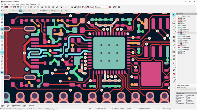
Import and Place Components
Update PCB from schematic (F8). All components appear in a cluster.
Place the USB connector on the top edge of the board, centered, with the plug side extending slightly beyond the board edge.
Place U2 (LDO) near the USB connector. Put C7 and C8 immediately adjacent to its input and output pins.
Place U1 (ATmega328P-AU) in the center. The TQFP package is compact, so component placement around it matters more.
Place the crystal (Y1) as close to pins 7 and 8 as possible. Place C1 and C2 right next to the crystal.
Place decoupling caps (C3, C4) within 3mm of the VCC/AVCC pins. Shorter is better.
Place sensors. Put U3 (SHT30) away from heat sources (the LDO, MCU). Temperature sensors need accurate ambient readings. Put U4 (VEML7700) near a board edge where it can see ambient light.
Place the ISP header (J2) and UART header (J3) on the bottom edge for easy access.
Place the reset button near a board edge.
Routing Strategy
Route power traces first using the Power net class (0.5mm). Run +5V and +3V3 as short, direct traces from their sources to each component.
Route the crystal traces. Keep XTAL1 and XTAL2 short, symmetric, and away from other signals. Guard them with a ground pour later.
Route I2C bus. SDA and SCL run from the MCU to both sensors and the pull-up resistors. Keep these traces under 50mm total length. Route them as a pair with consistent spacing.
Route UART. TX and RX from the MCU to the UART header. These are low-speed signals, so routing is straightforward.
Route ISP signals. MISO, MOSI, SCK, RESET from the MCU to the ISP header.
Use vias when needed. With a double-sided board, you can route signals on the back copper layer. Press V during routing to place a via and switch layers. Keep via count reasonable (under 20 for this board).
Add ground pours on both layers. Create a GND zone on F.Cu and B.Cu. Fill them with B (Build All Zones). This provides a solid ground plane and reduces the amount of copper that needs to be removed during milling.
Run DRC. Zero errors, zero unconnected items.
Optional: Speed Up With Freerouting
KiCad does not ship a built-in autorouter (the original was Java-based and dropped in KiCad 5 because no one stepped up to maintain it). The community-standard replacement is Freerouting, a free Java app that talks to KiCad through the Specctra DSN/SES file format.
For a board this dense, Freerouting can save real time, but only if you do not let it touch the nets that matter:
Hand-route and lock the critical nets first. Power (+5V, +3V3, GND), the crystal pair (XTAL1/XTAL2), and the I2C pair (SDA/SCL) all benefit from deliberate placement. Route them yourself, then select each track and check Locked in the Properties panel. Locked tracks survive the autorouter pass.
Install Freerouting. Download the latest release from github.com/freerouting/freerouting (you need a Java runtime installed). On many systems it is also available through KiCad’s Plugin and Content Manager (PCM).
Launch the autorouter from the PCB Editor toolbar (the icon usually looks like a maze or a green PCB with arrows). The dialog exports a .dsn of the current board, hands it to Freerouting, waits for results, and imports the .ses back automatically.
Review the result. Look for: too many vias on a single net, sharp corners on signals you care about, traces that cross under the crystal. Re-route by hand anything you don’t like; the autoroute is a starting point, not a finished design.
Run DRC again. Locked tracks should be untouched, the rest should be connected, zero errors.
For a small, mostly-digital board like this one, hand routing teaches you more and the time difference is small. Freerouting earns its place when you reach 50+ nets, are working under deadline, or routing pure digital fan-out where aesthetics matter less than completion. Either choice produces the same Gerbers downstream.
Double-Sided Layout Tips
SMD Placement Rules
Keep all SMD components on the front side unless space forces some to the back
Through-hole components (ISP header, UART header) can go on either side
If a component must go on the back, flip it with F key in KiCad
The sensor ICs (SHT30, VEML7700) should face outward, not trapped between the board and a surface
Manufacturing: CNC Milling
CNC milling removes copper mechanically instead of chemically. A small end mill cuts isolation channels around traces, leaving the copper traces as raised islands. This works well for double-sided boards because you can flip the board and mill the other side.
Why CNC Milling?
No chemicals (no ferric chloride, no disposal issues)
Higher precision than toner transfer (0.1mm channels are achievable)
Repeatable (once set up, you can make identical boards)
Drills holes in the same setup
Works well for fine-pitch SMD pads like TQFP
CNC Milling Workflow
Export Gerber files. In KiCad PCB Editor, go to File > Plot. Select F.Cu, B.Cu, and Edge.Cuts layers. Set format to Gerber. Click Plot. Then click Generate Drill Files in Excellon format.
Import into your CNC software. Common options:
FlatCAM (free, open source): imports Gerbers and generates G-code
Candle or bCNC: G-code senders for GRBL-based CNC machines
PCB-GCODE (Eagle plugin also works with Gerber conversions)
Set milling parameters in FlatCAM:
V-bit: 0.1mm tip, 30-degree angle
Isolation width: 0.15mm (number of passes: 2-3 for wider isolation)
Feed rate: 100-200 mm/min
Cut depth: 0.05-0.1mm (just deep enough to cut through the copper layer, typically 35 µm thick)
Secure the copper-clad board to the CNC bed. Use double-sided tape or a vacuum table. The board must be perfectly flat; any warping will cause uneven cuts.
Set the Z-origin (tool height). Touch the bit to the board surface. A Z-probe or continuity tester helps find the exact surface. This is the most critical setup step: too shallow and traces short together, too deep and the bit wears out fast.
Mill the front copper layer. Run the F.Cu isolation routing G-code. The CNC cuts channels around every pad and trace, leaving copper islands.
Drill all holes. Switch to a 0.8mm drill bit and run the Excellon drill file. The holes serve as alignment points when you flip the board.
Flip the board for the back layer. Use two drilled holes as alignment pins. Secure the board face-down. Re-probe the Z-height.
Mill the back copper layer. Run the B.Cu isolation routing G-code.
Mill the board outline. Switch to a 1-2mm end mill and run the Edge.Cuts G-code to cut the board to its final shape.
Clean and inspect. Remove copper dust with a brush. Inspect under magnification: check that all isolation channels are clean and no copper bridges remain between pads.
Connecting Front and Back Layers (Manual Vias)
CNC-milled boards do not have plated through-holes. You need to create manual vias:
For each via, insert a short piece of bare copper wire (0.5mm diameter) through the drilled hole.
Solder the wire to the pad on the front side, trim it, then flip the board and solder it to the pad on the back side.
Trim excess wire flush with the solder joints.
This adds time compared to professionally fabricated boards, but it works reliably for prototypes.
Soldering SMD Components
SMD soldering requires different tools than through-hole work.
Tools Needed
Tool
Purpose
Fine-tip soldering iron (0.5mm tip)
Resistors, capacitors, LED, headers
Solder paste (Sn63/Pb37 or lead-free)
TQFP and sensor ICs
Hot air station
Reflowing solder paste on TQFP and sensors
Flux pen
Improving solder flow on fine-pitch pads
Tweezers (fine-point)
Placing 0805 components
Magnifying glass or microscope
Inspecting solder joints
Soldering Order
TQFP MCU first. Apply solder paste to the TQFP-32 pads. Place the ATmega328P-AU with tweezers, aligning pin 1 with the pad 1 mark. Reflow with hot air at 250-280°C, holding the nozzle 2-3 cm above the chip. The paste will melt and self-align the chip. Inspect every pin under magnification for solder bridges.
Sensor ICs. Apply paste and reflow the SHT30 and VEML7700 the same way. The SHT30 has an exposed pad on the bottom; make sure the paste connects it to the ground pad.
LDO and crystal. Solder the SOT-223 regulator and SMD crystal. These are larger and easier than the sensors.
0805 passives. Tin one pad of each resistor/capacitor location with a small amount of solder. Place the component with tweezers, reflow the tinned pad, then solder the other pad. This “tack and solder” method is fast for 0805 parts.
USB connector. Solder the Micro-B connector. The shield pins provide mechanical strength; solder them well.
Through-hole headers. Solder the ISP and UART pin headers last, as they are the tallest components.
Manual vias. If you used CNC milling, solder all via wires now.
Common SMD Mistakes
Troubleshooting
Solder bridges on TQFP: drag a clean, fluxed iron tip across the pins to wick away excess solder. Or use solder wick.
Tombstoning (0805 part stands up on one end): uneven solder paste or uneven heating. Remove, clean, and resolder.
Cold joints: dull, grainy appearance. Reheat with flux.
Component shifted during reflow: the component moved when you applied hot air. Use less airflow, or tack one side with an iron first.
First Power-On and Testing
Visual inspection. Check every solder joint under magnification. Look for bridges on the TQFP pins especially.
Continuity check. Verify no short between +5V and GND, or +3V3 and GND.
Apply power via USB. Plug in a USB cable. The power LED should light. Measure +5V at the MCU VCC pin and +3.3V at the sensor VDD pins.
Flash the blink firmware from Lesson 1 over the ISP header. If the LED blinks, the MCU and crystal are working.
Firmware: Reading Sensors
Save this as sensor_read.c. It reads both I2C sensors and outputs data over UART at 9600 baud.
/*
* sensor_read.c - Read SHT30 and VEML7700 via I2C, output via UART
Comments