A development board running an ESP32 draws 40 to 80 mA even in idle, which drains a small lithium cell in a day or two. For a sensor node deployed outdoors or in a hard-to-reach location, you need a purpose-built board where every component is chosen for minimal quiescent current: a low-Iq LDO instead of a dev board’s wasteful regulator, a charging IC that can top up from a solar panel, and a layout that keeps leakage paths short. In this lesson you will design that board around the ESP32-C3-MINI-1, with TP4056 lithium charging, solar input, battery protection, and a power budget targeting months of operation on a single cell. #KiCad #ESP32 #IoT
  Power System Block Diagram  ──────────────────────────────────────────  Solar Panel ──►┐  (5V, 200mA)    │                 ▼  USB-C (5V) ──► TP4056 ──► DW01A + 8205A                 (charger)  (battery protection)                     │           │                     ▼           ▼                 Li-Po Battery (3.7V, 1000mAh)                     │                     ▼                 ME6211 LDO ──► 3.3V rail                 (Iq ~40uA)      │                                 ├──► ESP32-C3                                 └──► BME280
  Deep sleep: ESP32 ~5uA + LDO ~40uA            = ~45uA total board current
What We Are Building
Battery-Powered ESP32-C3 IoT Sensor Node
A compact wireless sensor node that monitors temperature, humidity, and barometric pressure using a BME280. The ESP32-C3 wakes from deep sleep every 10 minutes, reads the sensor, transmits data over WiFi or BLE, and returns to sleep. A TP4056 charges the lithium battery from USB-C or a small solar panel. The entire board targets under 10 µA sleep current for months of autonomous operation.
The power system is the heart of any battery-operated design. A poorly designed power path can drain a battery in days. This section covers each stage of the power chain, from charging through regulation, and explains how each component contributes to the total sleep current budget.
Battery Charging: TP4056
The TP4056 is a complete constant-current, constant-voltage linear charger for single-cell lithium batteries. It charges to 4.2V and automatically terminates when the charge current drops below a threshold (typically 1/10 of the programmed current).
Key connections:
PROG pin: A resistor from PROG to GND sets the charge current. For 500 mA charging, use a 2 kΩ resistor. For solar charging with a small panel (100 mA), you might use a 10 kΩ resistor instead.
VIN: Connect to the USB-C VBUS or solar panel output through the diode-OR network.
BAT: Connect to the battery through the DW01A protection circuit.
CHRG and STDBY: Open-drain outputs that drive the charging and standby indicator LEDs.
Charge current reference:
PROG Resistor
Charge Current
10 kΩ
130 mA
5 kΩ
250 mA
2 kΩ
500 mA
1.2 kΩ
830 mA
1 kΩ
1000 mA
Solar and USB Input: Diode-OR
The board accepts power from either USB-C or a solar panel. A diode-OR network using two Schottky diodes (SS14) connects both sources to the TP4056 VIN pin. Whichever source has the higher voltage forward-biases its diode and supplies current. The Schottky diodes have low forward voltage drop (~0.3V), minimizing power loss.
The circuit is straightforward:
USB VBUS connects through D2 (SS14) to TP4056 VIN.
Solar panel output connects through D1 (SS14) to TP4056 VIN.
A 10 µF capacitor on VIN smooths the input.
When both sources are present, USB typically wins because the solar panel open-circuit voltage is usually around 5 to 6V and drops under load, while USB provides a stable 5V.
Battery Protection: DW01A + 8205A
The DW01A is a lithium battery protection IC that monitors the cell voltage and current. It controls the 8205A, a dual N-channel MOSFET that sits in the battery’s ground path. Together they protect against three failure modes.
Protection
Threshold
Action
Overcharge
~4.3V
Disconnects charge path
Overdischarge
~2.4V
Disconnects load
Overcurrent
~3A
Disconnects load
The DW01A connects between B+ and B- of the battery. Its OD and OC pins drive the gates of the two MOSFETs in the 8205A. The 8205A sits between the battery negative terminal and system ground. When a fault is detected, the appropriate MOSFET turns off, disconnecting the battery.
Voltage Regulation: ME6211 LDO
The ME6211C33M5G provides a stable 3.3V output from the battery voltage (3.0V to 4.2V). Its key advantage for battery applications is the very low quiescent current, approximately 40 µA. This is the current the regulator itself consumes even when the load draws nothing. For a broader look at LDO selection, switching regulators, and power rail design, see Analog Electronics: Power Supply Design.
Input: Battery voltage (3.0V to 4.2V from the protected output)
Output: 3.3V, up to 500 mA
Dropout voltage: ~100 mV at light loads
Input capacitor: 10 µF ceramic
Output capacitors: 10 µF ceramic + 100 nF ceramic
Power Budget Calculation
Understanding your total sleep current is critical for estimating battery life. Every component that remains powered during deep sleep contributes to the total.
Component
Sleep Current
Notes
ESP32-C3 deep sleep
~5 µA
RTC memory retained
BME280 sleep mode
~0.1 µA
Powered off via MOSFET: 0 µA
ME6211 quiescent
~40 µA
Always on
TP4056 standby
~2 µA
Battery full, no input
DW01A + 8205A
~3 µA
Protection circuit
Pull-up/pull-down resistors
~1 µA
Depends on values chosen
Total sleep current
~51 µA
Conservative estimate
Battery life estimate with a 500 mAh cell:
Sleep current: ~51 µA
Wake current: ~80 mA for WiFi TX, ~5 mA for sensor read
Wake duration: ~5 seconds every 10 minutes (0.83% duty cycle)
Average current: 51 µA + (80 mA x 0.0083) ≈ 51 µA + 664 µA ≈ 715 µA
Battery life: 500 mAh / 0.715 mA ≈ 699 hours ≈ 29 days with WiFi
For BLE-only transmission (peak ~15 mA, wake ~2 seconds):
Average current: 51 µA + (15 mA x 0.0033) ≈ 51 µA + 50 µA ≈ 101 µA
Battery life: 500 mAh / 0.101 mA ≈ 4950 hours ≈ 206 days
With a small solar panel providing even modest charging on sunny days, the system can run indefinitely.
Deep Sleep Considerations for PCB Design
Designing for low sleep current is not just a firmware problem. The PCB itself can waste microamps through pull-up resistors, indicator LEDs, and always-on peripherals. This section covers the hardware design choices that make deep sleep effective.
Resistor Values Matter
Every pull-up or pull-down resistor that connects a voltage rail to ground (through a GPIO or other node) creates a constant current leak. For a 3.3V rail:
Resistor Value
Leak Current
4.7 kΩ
702 µA
10 kΩ
330 µA
47 kΩ
70 µA
100 kΩ
33 µA
Rules for battery-powered designs:
Use 100 kΩ or higher for pull-ups/pull-downs where possible
I2C pull-ups: use 10 kΩ instead of the common 4.7 kΩ. At 100 kHz I2C clock speed, 10 kΩ works reliably for short bus lengths (under 10 cm on a PCB)
The EN pin pull-up on the ESP32-C3 can be 100 kΩ with a 1 µF capacitor for slow rise time
LED Power Waste
A typical indicator LED draws 5 to 20 mA. If a power LED stays on during deep sleep, it dominates the entire current budget. Solutions:
Remove the power LED entirely (simplest approach for deployed sensor nodes)
Add a solder jumper in series with the LED, so you can cut the trace after debugging
Gate the LED with a MOSFET controlled by a GPIO (only illuminate when the processor is awake)
In this design, the TP4056 CHRG and STDBY LEDs only illuminate during charging, so they do not affect sleep current when running on battery alone.
Switchable Sensor Power
The BME280 draws about 0.1 µA in sleep mode, which is negligible. However, for sensors that draw more idle current, or to ensure a clean sensor startup, you can switch the sensor’s power rail using a P-channel MOSFET controlled by a GPIO.
The circuit uses a SI2301 P-MOSFET:
Source: 3.3V rail
Drain: Sensor VCC (BME280 VDD)
Gate: GPIO pin through a 100 kΩ pull-up to 3.3V
When the GPIO drives LOW, the MOSFET turns on and powers the sensor. When the GPIO is HIGH (or floating during deep sleep with the pull-up), the MOSFET turns off and the sensor draws zero current.
USB-UART Bridge Current
Many ESP32 development boards include a CP2102 or CH340 USB-to-UART bridge chip. These draw 5 to 15 mA even when idle, which destroys battery life. The ESP32-C3 has native USB support built into the chip, eliminating the need for an external bridge. This saves board space, BOM cost, and significant sleep current.
Schematic Capture
Open KiCad 9 and create a new project named “esp32c3-iot-sensor”. The schematic has five functional blocks: USB-C input, battery charging and protection, voltage regulation, ESP32-C3 module, and the BME280 sensor with switchable power. Lay out each block in its own area of the schematic sheet.
For a power and programming connection, you only need VBUS, GND, D+, D-, CC1, and CC2. Place two 5.1 kΩ resistors from CC1 and CC2 to GND. These tell the USB host that this is a device requesting default USB power (5V, up to 500 mA).
Connect VBUS through Schottky diode D2 to the TP4056 VIN net.
Connect the USB data lines
The ESP32-C3 native USB pins are GPIO18 (D-) and GPIO19 (D+). Route these directly from the USB-C connector to the module pins. No external components are needed; the ESP32-C3 handles USB internally.
TP4056 Charging Circuit
Place the TP4056 IC
Connect VIN to the diode-OR output from USB and solar. Place a 10 µF input capacitor close to the VIN pin.
Set the charge current
Place a 2 kΩ resistor from the PROG pin to GND. This programs a 500 mA charge current. If using a small solar panel as the primary source, consider 10 kΩ (130 mA) to match the panel’s output capability.
Add status LEDs
Connect CHRG to LED1 (red) through a 1 kΩ resistor to VIN. Connect STDBY to LED2 (green) through a 1 kΩ resistor to VIN. Both pins are open-drain, so they sink current through the LEDs.
Connect BAT to the protection circuit
The TP4056 BAT pin connects to the positive terminal of the DW01A protection circuit (B+ net).
Solar Panel Input
Place the solar panel connector (J3)
Use a JST-PH 2-pin connector. Connect the positive pin through Schottky diode D1 to the TP4056 VIN net (same net as the USB diode output).
Add reverse polarity protection
The Schottky diode D1 also prevents current from flowing back into the solar panel when USB is connected or the battery voltage exceeds the panel voltage.
Battery Protection Circuit
Place the DW01A
Connect VCC to B+ (battery positive). Connect VSS to the drain of the low-side MOSFET in the 8205A. The OD (overdischarge) and OC (overcharge/overcurrent) pins connect to the gates of the two MOSFETs in the 8205A.
Place the 8205A dual MOSFET
The 8205A contains two N-channel MOSFETs in series. Connect the source of one MOSFET to the battery negative terminal (B-). Connect the drain of the other MOSFET to system ground (GND). The gates connect to the DW01A OD and OC pins.
Add the current sense resistor path
Place a 100 kΩ resistor from the DW01A CS pin to the junction between the two MOSFETs. This is the current sense input for overcurrent detection.
Battery Connector
Place a JST-PH 2-pin connector (J2) for the battery. Connect the positive pin to B+ (feeding into the DW01A protection). Connect the negative pin to B- (battery ground, before the protection MOSFETs).
ME6211 LDO
Place the ME6211C33M5G
Connect VIN to the protected battery output (the system side of the 8205A, which is the node between the TP4056 BAT pin and the load). Place a 10 µF input capacitor close to VIN.
Add output capacitors
Place a 10 µF ceramic and a 100 nF ceramic on the 3.3V output, close to the VOUT pin. The ME6211 requires at least 1 µF output capacitance for stability.
Connect EN
Tie the enable pin directly to VIN so the regulator is always on when battery voltage is present.
ESP32-C3-MINI-1 Module
Place the module
The ESP32-C3-MINI-1 has castellated pads around its edges and a large ground pad underneath. Connect VCC (pin 2) to the 3.3V rail. Connect all GND pins and the exposed pad to GND.
Add decoupling
Place a 10 µF bulk capacitor and a 100 nF capacitor close to the VCC pin.
EN (enable) circuit
Connect a 100 kΩ pull-up resistor from EN to 3.3V. Add a 1 µF capacitor from EN to GND for a slow rise time, which ensures reliable startup. Connect the reset button (SW1) between EN and GND.
Boot button
Connect SW2 between GPIO9 and GND. Holding GPIO9 low during reset puts the ESP32-C3 into download mode for flashing firmware over USB.
I2C pins for BME280
Assign GPIO4 as SDA and GPIO5 as SCL. Place 10 kΩ pull-up resistors from each to the 3.3V rail.
Sensor power control
Assign GPIO3 as the sensor power control pin. Connect it to the gate of the P-MOSFET (Q2) through a 100 Ω gate resistor for EMI damping.
BME280 Sensor
Place the BME280
The BME280 comes in a tiny LGA-8 package (2.5 x 2.5 mm). Connect VDD to the switched 3.3V rail (drain of Q2). Connect GND to ground. Place a 100 nF decoupling capacitor close to VDD.
Set the I2C address
Connect the SDO pin to GND for I2C address 0x76, or to VDD for address 0x77. GND is the more common choice.
Connect I2C
Connect SDA to GPIO4 and SCL to GPIO5 on the ESP32-C3. The pull-up resistors are already on the main 3.3V rail, which means I2C communication works even when the sensor power MOSFET is off (the pull-ups hold the lines high).
CSB pin
Connect CSB to VDD (the switched rail) to select I2C mode. If CSB is left floating, the BME280 may enter SPI mode.
Run ERC and Assign Footprints
Run Electrical Rules Check
Fix any unconnected pins, missing power flags, or conflicting outputs. Add power flags on the battery input net and USB VBUS net if KiCad reports them as undriven.
Assign footprints
Use the footprint assignment tool to map each symbol to its physical package. The ESP32-C3-MINI-1 footprint may need to be downloaded from Espressif’s KiCad library or the SnapEDA/Ultra Librarian services.
Generate the netlist
Export the netlist and open the PCB editor.
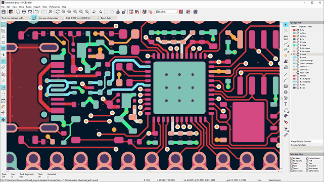
PCB Layout
The PCB layout for a battery-powered IoT node requires careful attention to three areas: antenna clearance for the ESP32-C3, thermal management for the TP4056 charger, and short power paths for low impedance. The target board size is 45 x 30 mm on a 2-layer PCB.
Board Setup
Set the board outline
Draw a 45 x 30 mm rectangle on the Edge.Cuts layer. Add rounded corners with a 1 mm radius for a cleaner look and easier handling.
Configure design rules
Set minimum trace width to 0.15 mm, minimum clearance to 0.15 mm. For power traces (VBAT, 3.3V, GND), use 0.4 mm or wider. USB data traces can use 0.25 mm.
Set up the ground pour
Plan for copper fills on both front and back layers connected to GND. Do not pour them yet; wait until all traces are routed.
Component Placement
Place the ESP32-C3-MINI-1 module
Position it along one short edge of the board with the antenna extending past the board edge or flush with it. The antenna end must have no copper on any layer within 2 mm of the antenna area.
Place the USB-C connector
Position it on the opposite short edge from the antenna. This keeps the USB cable away from the antenna, reducing interference.
Place the TP4056 and protection circuit
Group the TP4056, DW01A, 8205A, and their associated passives near the USB-C connector and battery connector. The TP4056 dissipates heat during charging (up to ~1.5W at 500 mA from 5V to a 3.7V battery), so place it with access to a copper pour for heat spreading.
Place the battery and solar connectors
Position J2 (battery) and J3 (solar) along one long edge of the board. Through-hole JST connectors need clearance for the housing.
Place the ME6211 LDO
Position it between the charging/protection section and the ESP32-C3. Keep input and output capacitors within 3 mm of the IC.
Place the BME280
Position it away from the TP4056 and LDO to avoid heat from those components affecting temperature readings. The ideal location is near the board edge, far from heat sources. Consider adding a routed slot or thermal relief cutout in the PCB between the sensor and the power section.
Place buttons and LEDs
Position the reset and boot buttons where they are accessible. Place the charging LEDs near the USB connector.
Antenna Keepout Zone
In KiCad, draw a keepout area on both copper layers covering the antenna region. Set the keepout to prohibit copper fills and tracks. The Espressif datasheet specifies the exact dimensions.
Thermal Management for TP4056
The TP4056 in SOP-8 package does not have an exposed thermal pad, so it relies on the PCB copper for heat dissipation. During charging at 500 mA from a 5V source into a 3.7V battery, the IC dissipates approximately:
P = (5V - 3.7V) x 0.5A = 0.65W
This is manageable, but the copper area around the thermal pad and GND pins should be as large as practical. Connect the GND pad to a wide copper pour on both layers with multiple vias.
Routing Guidelines
Route power traces first
Start with VBAT, 3.3V, and GND. Use 0.4 mm or wider traces. Keep the path from the LDO output to the ESP32-C3 VCC short and direct.
Route USB data lines
Keep D+ and D- as a parallel pair with consistent spacing. Match their lengths to within 0.5 mm. Avoid routing them near switching signals or the antenna.
Route I2C lines
SDA and SCL to the BME280. These are low-speed signals, so routing is straightforward. Keep them reasonably short and away from the antenna area.
Fill copper zones
Pour ground fills on both front and back layers. Add vias to stitch the ground planes together, especially near the ESP32 module ground pad and the TP4056 ground area.
Run DRC
Check for clearance violations, unrouted nets, and minimum width errors. Fix any issues before generating Gerbers.
Manufacturing
Export Gerbers and drill files from KiCad using File, then Plot. Select all copper layers (F.Cu, B.Cu), silkscreen layers, mask layers, and Edge.Cuts. Generate the drill file in Excellon format. Compress all files into a single ZIP.
Upload to JLCPCB or your preferred fabricator. For this 2-layer board, standard settings work well:
Parameter
Setting
Layers
2
PCB thickness
1.6 mm
Surface finish
HASL (lead-free) or ENIG
Copper weight
1 oz
Solder mask
Green (or your preference)
Min trace/space
6/6 mil (0.15/0.15 mm)
Order a stencil for the top layer if you plan to reflow solder the QFN and LGA components. The BME280 in LGA-8 and the 8205A in TSSOP-8 are much easier to solder with paste and hot air or a reflow oven than by hand.
Firmware: Deep Sleep Sensor Reading
The firmware demonstrates the core IoT sensor pattern: wake up, read sensors, transmit data, go back to sleep. This example uses the Arduino framework for the ESP32-C3, reads the BME280 over I2C, prints the data to USB serial, and enters deep sleep for 10 minutes.
Arduino Setup
Install the ESP32 board package in Arduino IDE (or PlatformIO). Select “ESP32C3 Dev Module” as the board. Install the Adafruit BME280 library and the Adafruit Unified Sensor library from the Library Manager.
Complete Sketch
#include<Wire.h>
#include<Adafruit_Sensor.h>
#include<Adafruit_BME280.h>
// Pin definitions
#defineSDA_PIN4
#defineSCL_PIN5
#defineSENSOR_POWER_PIN3
// Deep sleep duration: 10 minutes in microseconds
#defineSLEEP_DURATION_US600000000ULL
// BME280 I2C address (SDO to GND = 0x76)
#defineBME280_ADDR0x76
Adafruit_BME280 bme;
voidsetup() {
// Initialize USB serial
Serial.begin(115200);
delay(100);
// Power on the BME280 sensor
pinMode(SENSOR_POWER_PIN, OUTPUT);
digitalWrite(SENSOR_POWER_PIN, LOW); // P-MOSFET: LOW = ON
// Wait for sensor power to stabilize
delay(50);
// Initialize I2C
Wire.begin(SDA_PIN, SCL_PIN);
// Initialize BME280
if (!bme.begin(BME280_ADDR, &Wire)) {
Serial.println("BME280 not found. Check wiring.");
digitalWrite(SENSOR_POWER_PIN, HIGH); // P-MOSFET: HIGH = OFF
// Go to deep sleep
goToSleep();
}
voidgoToSleep() {
Serial.println("Entering deep sleep for 10 minutes...");
Serial.flush();
// Configure deep sleep timer
esp_sleep_enable_timer_wakeup(SLEEP_DURATION_US);
// Enter deep sleep
esp_deep_sleep_start();
}
voidloop() {
// This never executes. After deep sleep,
// the ESP32-C3 resets and runs setup() again.
}
How It Works
The ESP32-C3 deep sleep mechanism resets the processor on wake. Execution always starts from setup(), not from where it left off. The RTC memory retains a small amount of data across sleep cycles if needed (for example, a boot counter or accumulated readings).
The firmware flow:
Wake from deep sleep (or initial power-on)
Drive GPIO3 LOW to turn on the sensor power MOSFET
Wait 50 ms for the sensor power rail to stabilize
Initialize I2C and the BME280
Take a forced measurement (single reading, lowest power)
Read temperature, humidity, and pressure
Print the data over USB serial
Drive GPIO3 HIGH to turn off the sensor
Enter deep sleep for 10 minutes
To add WiFi transmission, insert a WiFi connect and HTTP POST (or MQTT publish) between step 7 and step 8. WiFi adds approximately 3 to 5 seconds of wake time and 80 to 150 mA of current draw.
PlatformIO Alternative
If you prefer PlatformIO, create a project with the following platformio.ini:
[env:esp32c3]
platform = espressif32
board = esp32-c3-devkitm-1
framework = arduino
monitor_speed = 115200
lib_deps =
adafruit/Adafruit BME280 Library@^2.2.2
adafruit/Adafruit Unified Sensor@^1.1.9
The source code is identical. Place it in src/main.cpp.
What You Have Learned
Lesson 6 Complete
KiCad skills:
Designed a multi-source power input with diode-OR topology
Placed and connected a lithium battery charging circuit (TP4056) with protection (DW01A + 8205A)
Managed antenna keepout zones for the ESP32-C3 WiFi/BLE module
Applied thermal management techniques for power dissipation in the TP4056
Routed a compact 2-layer board with ground pours on both sides
Electronics skills:
Lithium battery charging, protection, and safety circuit design
Solar panel input integration with USB charging
Low-quiescent-current LDO selection for battery applications
Power budget analysis for deep sleep IoT devices
Switchable sensor power using P-channel MOSFETs
Firmware skills:
ESP32-C3 deep sleep with timer wakeup
BME280 forced mode measurement for lowest power consumption
GPIO-controlled sensor power switching
Arduino framework for ESP32-C3 with native USB serial
Comments