This lesson designs a development board around the Raspberry Pi RP2040, a dual-core ARM Cortex-M0+ microcontroller with Programmable I/O (PIO) hardware. Unlike every MCU in the previous lessons, the RP2040 has no internal flash. It boots entirely from an external QSPI flash chip, which introduces new routing constraints. You will work with a QFN-56 package, design a dual power domain (3.3V I/O and 1.1V core), and route high-speed QSPI traces on a 4-layer board. #KiCad #RP2040 #PIO
RP2040 Dual Power Domain
──────────────────────────────────────────
USB-C 5V ──► NCP1117 LDO ──► 3.3V (IOVDD)
│
┌──────────────┤
│ │
▼ ▼
┌─────────┐ ┌─────────────┐
│ RP2040 │ │ W25Q128 │
│ (IOVDD │ │ QSPI Flash │
│ = 3.3V) │ │ (3.3V) │
│ │ └─────────────┘
│ Internal │
│ 1.1V reg ├──► DVDD (core)
│ ┌───┐ │
│ │ L │ │ 1uH inductor
│ └───┘ │ + caps required
└──────────┘
What We Are Building
RP2040 USB-C Development Board with PIO
A Pico-style development board built around the RP2040 in a QFN-56 package. The board includes 16 MB of external QSPI flash, native USB-C (no USB bridge chip needed), a 12 MHz crystal for the USB PLL, 3.3V LDO regulation with the RP2040’s internal 1.1V core regulator, a WS2812B RGB LED, SWD debug header, BOOTSEL and reset buttons, and 2x20-pin GPIO headers with PIO-capable pins marked.
Board specifications:
Parameter
Value
MCU
RP2040 (QFN-56, 7x7mm, 0.4mm pitch, dual Cortex-M0+ at 133 MHz)
Flash
W25Q128JV 16 MB QSPI (or W25Q16JV 2 MB)
USB
USB-C, native USB 1.1 Full-Speed (device and host capable)
The RP2040 is the first microcontroller designed by Raspberry Pi. It packs two ARM Cortex-M0+ cores running at up to 133 MHz, 264 KB of on-chip SRAM (split into six banks), and a rich set of peripherals. What sets it apart from most microcontrollers is the Programmable I/O (PIO) subsystem: two PIO blocks, each containing four state machines that can execute small programs to implement custom I/O protocols entirely in hardware. PIO can generate precise timing for protocols like WS2812B LED control, VGA video output, or custom serial interfaces without using any CPU cycles.
The RP2040 has no internal flash memory. All code is stored on an external QSPI flash chip and is either executed in place (XIP) through a cache or copied to SRAM at boot. The chip’s boot ROM contains a UF2 bootloader: hold the BOOTSEL button while plugging in USB, and the board appears as a mass storage device. You drag and drop a .uf2 firmware file to program it. No special programmer or software is needed.
Native USB 1.1 is built into the RP2040, supporting both device and host modes. The USB PHY is internal, so the D+ and D- lines connect directly to the USB connector through series termination resistors. A 12 MHz crystal provides the reference clock for the USB PLL, which generates the 48 MHz USB clock internally.
Key RP2040 Features
Feature
Detail
Cores
2x Cortex-M0+ at 133 MHz
SRAM
264 KB (6 independent banks)
Flash
None (external QSPI required)
PIO
2 blocks, 4 state machines each, 32 instructions per block
USB
USB 1.1 device/host, internal PHY
GPIO
30 multi-function GPIO (all PIO-capable)
ADC
4-channel 12-bit SAR ADC + internal temperature sensor
PWM
16 channels (8 slices, 2 outputs each)
SPI
2x SPI controllers
I2C
2x I2C controllers
UART
2x UART
DMA
12-channel DMA controller
QFN Package Considerations
The RP2040 comes in a QFN-56 package measuring 7x7 mm with 0.4 mm pad pitch. QFN (Quad Flat No-lead) packages have no visible leads extending from the sides. Instead, the electrical connections are flat pads on the bottom of the package. This makes QFN packages compact and excellent for high-frequency performance (short bond wire lengths mean lower inductance), but it also means you cannot solder them with a standard soldering iron.
QFN Soldering Requirements
The QFN-56 has 56 perimeter pads plus a large exposed thermal/ground pad in the center. The exposed pad serves two critical functions: it provides the primary ground connection for the die, and it conducts heat away from the chip into the PCB. This pad must be soldered to the PCB ground plane.
What you need for QFN assembly:
Solder paste stencil. Order a stainless steel stencil with your PCBs. The stencil has laser-cut openings that match every pad on the board. You squeegee solder paste across the stencil, and paste deposits only where the pads are. For the QFN exposed pad, the stencil opening is typically divided into a grid pattern (for example, 3x3 or 4x4 smaller rectangles) to prevent excess paste from causing the chip to float during reflow.
Reflow soldering. After placing components on the pasted board, you reflow the entire assembly. Options include a hot air rework station (focused on the QFN area), a desktop reflow oven, or a modified toaster oven with a thermocouple and temperature controller. The reflow profile ramps to about 150 C for preheat, then peaks at 245 to 260 C for lead-free solder.
Placement accuracy. With 0.4 mm pitch pads, alignment matters. Use fine-tip tweezers and a magnifying lamp or microscope. The QFN package has a pin 1 indicator dot. Align it with the pin 1 marking on the PCB silkscreen. The self-centering effect of molten solder during reflow helps correct minor misalignment, but you need to be within about 0.1 mm.
PCB Pad Design for QFN
The KiCad footprint for the RP2040 QFN-56 should follow these guidelines:
Perimeter pads: Extend pads 0.2 mm beyond the package edge so you can visually inspect solder fillets from above. The pad width matches the QFN pad width (typically 0.2 mm for 0.4 mm pitch), and the pad length extends inward to just past the package edge.
Exposed pad: The PCB pad matches the exposed pad dimensions on the datasheet (approximately 3.1 x 3.1 mm for the RP2040). Apply a paste mask with a grid pattern to control solder volume.
Thermal vias: Place an array of small vias (0.3 mm drill, 0.6 mm pad) within the exposed pad area, connecting it to the inner ground plane. A 3x3 or 4x4 grid works well. These vias transfer heat from the QFN ground pad into the internal copper layers. Tent or plug the vias from the bottom side to prevent solder wicking through during reflow.
Schematic Capture
The RP2040 minimal circuit requires careful attention to multiple power domains and specific pin configurations. This section walks through each subsystem.
IOVDD (3.3V): Powers all GPIO and digital I/O. Six IOVDD pins, each needing a 100 nF decoupling capacitor placed within 2 mm of the pin.
DVDD (1.1V core): Powers the processor cores, SRAM, and internal logic. The RP2040 includes an internal voltage regulator that steps 3.3V (on VREG_VIN) down to 1.1V (on VREG_VOUT). This regulator requires an external 1 µH inductor and capacitors.
VREG_VOUT: connect through 1 µH inductor to DVDD, with 100 nF and 1 µF capacitors to ground
The inductor must be low DCR (under 0.5 Ω) to avoid excessive voltage drop
USB-C Connection
The RP2040 has a built-in USB PHY, so no external USB bridge chip is needed. The connections are straightforward:
USB-C Pin
Connection
VBUS
5V rail through polyfuse F1
CC1
5.1 kΩ to GND (identifies as UFP/device)
CC2
5.1 kΩ to GND
D+
27 Ω series resistor to RP2040 USB_DP (pin 47)
D-
27 Ω series resistor to RP2040 USB_DM (pin 46)
GND
Board ground
The 5.1 kΩ resistors on CC1 and CC2 tell the USB-C host that this board is a device requesting 5V default power. The 27 Ω series resistors on D+/D- provide impedance matching and ESD damping.
QSPI Flash Connection
The W25Q128JV connects to the RP2040’s dedicated QSPI pins. These are not regular GPIO; they are hardwired in the RP2040 for boot flash access.
Flash Pin
RP2040 Pin
Function
CLK
QSPI_SCLK
Clock
CS#
QSPI_SS
Chip select (active low)
DI (IO0)
QSPI_SD0
Data in / IO0
DO (IO1)
QSPI_SD1
Data out / IO1
WP# (IO2)
QSPI_SD2
Write protect / IO2
HOLD# (IO3)
QSPI_SD3
Hold / IO3
VCC
3.3V
Power (100 nF + 4.7 µF decoupling)
GND
GND
Ground
Add a 1 kΩ pull-up resistor on CS# to 3.3V to ensure the flash is deselected during power-up before the RP2040 takes control.
Crystal Oscillator
The 12 MHz crystal connects between XIN (pin 22) and XOUT (pin 23):
15 pF load capacitors from each pin to ground
Crystal should be placed as close to the RP2040 as possible (within 5 mm)
Guard the crystal traces with a ground pour to prevent interference
No traces should run between the two crystal pads
BOOTSEL and Reset
BOOTSEL button: This is connected to QSPI_SS (the flash chip select line). When QSPI_SS is held LOW during power-up or reset, the RP2040’s boot ROM enters UF2 mass storage mode instead of booting from flash. The button shorts QSPI_SS to GND. During normal operation, the button press is ignored because the RP2040 drives QSPI_SS as an output.
Reset button: The RUN pin is the RP2040’s active-low reset. Connect a 10 kΩ pull-up to 3.3V and a tactile switch to GND. Pressing the button pulls RUN low, resetting both cores.
To enter UF2 bootloader mode: hold BOOTSEL, press and release reset, then release BOOTSEL.
SWD Debug Header
The RP2040 supports Serial Wire Debug on dedicated pins:
SWDIO (pin 24)
SWCLK (pin 25)
GND
A 1x3 pin header is sufficient for basic SWD. Some debug probes (Raspberry Pi Debug Probe, Picoprobe) also use a UART connection, so you may optionally add a second header for UART0 TX/RX.
WS2812B RGB LED
The WS2812B is an addressable RGB LED with a built-in driver. It requires a single data line:
VDD: 3.3V (the WS2812B works at 3.5 to 5.3V; 3.3V is below the official minimum, but most units work reliably at 3.3V; alternatively, power from VBUS at 5V)
DIN: Connect to a GPIO (for example, GPIO16) through a 330 Ω series resistor
DOUT: Leave unconnected (only one LED in the chain)
GND: Board ground
Place a 100 nF decoupling capacitor between VDD and GND, close to the LED
GPIO Headers and PIO Pin Labeling
Break out all 26 available GPIO pins on two 1x20 headers (matching the Raspberry Pi Pico pinout where practical). The headers also carry 3.3V, GND, VBUS, and ADC_VREF.
All 30 GPIO on the RP2040 are PIO-capable. On the silkscreen, label the ADC-capable pins (GPIO26, GPIO27, GPIO28, GPIO29) with “ADC” to help users identify analog inputs. Label the SPI, I2C, and UART default pin assignments as well.
Electrical Rules Check
Run ERC in KiCad after completing the schematic:
Check power flags. Every power net (3.3V, 1.1V, VBUS, GND) must have a power flag symbol or be driven by a regulator output. The RP2040’s VREG_VOUT drives the 1.1V net, so mark it accordingly.
Verify unconnected pins. The RP2040 has several pins that must be connected to specific nets. TESTEN (pin 20) must be tied to GND. USB_VDD (pin 48) must be connected to 3.3V with a 100 nF decoupling capacitor. All six IOVDD pins must connect to 3.3V.
Check for missing decoupling. Each IOVDD pin pair and the DVDD pins should have associated 100 nF capacitors placed in the schematic.
Assign footprints. Open the footprint assignment tool and verify every component has the correct footprint. Pay special attention to the RP2040 QFN-56 footprint (should match the 7x7mm, 0.4mm pitch dimensions) and the W25Q128JV SOIC-8 footprint.
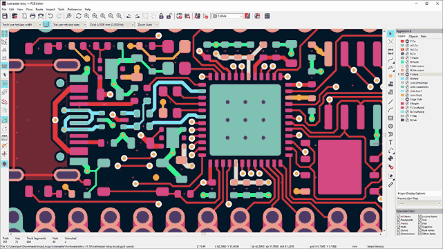
PCB Layout: 4-Layer Design
Layer Stackup
Use the same stackup proven in Lesson 4:
Layer
Function
Copper Weight
F.Cu (Layer 1)
Signal routing, component pads
1 oz
In1.Cu (Layer 2)
Ground plane (solid, unbroken)
0.5 oz
In2.Cu (Layer 3)
3.3V power plane
0.5 oz
B.Cu (Layer 4)
Signal routing, bottom components
1 oz
The ground plane on Layer 2 provides a continuous return path for all signals on Layer 1. The 3.3V plane on Layer 3 distributes power to all components through short vias. The 1.1V core supply is a small local pour near the RP2040, not a full-board plane.
QFN Pad Layout and Thermal Vias
Place the RP2040 near the center of the board, rotated so that the QSPI pins face the flash chip location and the USB pins face the board edge where the USB-C connector sits. The QFN exposed pad connects to GND through the PCB. Under this pad, create an array of thermal vias (3x3 or 4x4 grid, 0.3 mm drill) connecting F.Cu directly to the In1.Cu ground plane. In KiCad, you can add these vias inside the exposed pad copper zone. Set the via annular ring to 0.15 mm minimum to comply with standard fabrication rules.
On the solder paste layer, divide the exposed pad into a grid of smaller rectangles (for example, 9 rectangles in a 3x3 pattern) with gaps between them. This prevents too much solder paste from pooling under the chip, which could cause the RP2040 to float off the perimeter pads during reflow.
QSPI Flash Routing
The QSPI interface runs at up to 133 MHz (the W25Q128JV maximum). At these frequencies, trace length and matching matter.
QSPI routing rules:
Rule
Target
Maximum trace length (any QSPI signal)
25 mm
Length matching (all 6 signals within)
5 mm of each other
Routing layer
Single layer preferred (F.Cu), avoid vias
Trace width
0.15 to 0.2 mm (standard signal)
Spacing from other signals
At least 0.2 mm (2x trace width)
Series termination (optional)
33 Ω on CLK and IO0-IO3
Place the flash chip close to the RP2040. Position the W25Q128JV within 10 mm of the RP2040 QSPI pins, on the same side of the board. Shorter traces mean better signal integrity and easier length matching.
Route all six QSPI signals on F.Cu. Avoid layer transitions (vias) on the QSPI bus. Each via adds approximately 0.5 nH of inductance and breaks the return path on the ground plane. Keep all six traces (CLK, CS, IO0 through IO3) on the top layer.
Match trace lengths. In KiCad, use the interactive router’s length tuning tool. Select all six QSPI nets, set a target length (for example, 15 mm), and add serpentine meanders to shorter traces until all six are within 5 mm of the longest. The CLK trace is the most critical reference, so match data traces to the CLK length.
Add series termination resistors (optional). Place 33 Ω resistors in series with CLK and each data line, located close to the RP2040 pins (within 3 mm). These damp reflections and clean up signal edges. They are optional at lower clock speeds but recommended if you plan to run the flash at maximum speed.
Ground guard. Ensure a solid ground pour surrounds the QSPI traces on F.Cu, and the ground plane on In1.Cu is unbroken beneath the entire QSPI routing area.
USB Differential Pair Routing
The USB D+/D- pair requires 90 Ω differential impedance, the same technique covered in Lesson 4:
Route as a tightly coupled differential pair on F.Cu
Keep the pair on one layer (no vias)
Maintain continuous ground plane on In1.Cu beneath the traces
Trace width and spacing depend on your stackup geometry (use the KiCad impedance calculator or your fab’s stackup tool; typically ~0.2 mm trace width with ~0.15 mm gap for 90 Ω differential on a standard 4-layer 1.6 mm board)
Length match D+ and D- within 0.15 mm
Keep the total USB trace length under 50 mm
Place the 27 Ω series resistors at the RP2040 end, within 5 mm of the MCU pads
Crystal Routing
The 12 MHz crystal should be placed within 5 mm of the XIN/XOUT pins:
Route XIN and XOUT traces as short as possible (under 5 mm each)
Do not route any other signal between the crystal pads
Surround the crystal traces with a ground pour on F.Cu
Ensure the ground plane on In1.Cu is solid beneath the crystal area
Use 0.2 mm or wider traces for the crystal connections
Decoupling Capacitor Placement
Every power pin on the RP2040 needs a decoupling capacitor placed within 2 mm of the pin. The RP2040 has six IOVDD/IOVSS pin pairs and two DVDD/DVSS pin pairs. Place a 100 nF 0402 capacitor next to each pair. The via from the capacitor pad to the ground plane should be as short as possible (ideally directly adjacent to the pad).
For the core voltage regulator, place the 1 µH inductor and its associated capacitors (1 µF on VREG_VIN, 100 nF + 1 µF on VREG_VOUT) within 5 mm of the VREG pins. The inductor, capacitors, and RP2040 VREG pins form a tight loop. Keep this loop area small to minimize radiated EMI from the switching regulator.
The USB_VDD pin (pin 48) powers the internal USB PHY. Place a 100 nF capacitor directly at this pin with a short via to the ground plane.
Via Stitching and Ground Pour
Complete the layout with:
Via stitching around the board perimeter and between ground pour islands (every 3 to 5 mm)
Ground pour on both F.Cu and B.Cu connected to the In1.Cu ground plane
Via stitching around the USB differential pair (ground vias on both sides, spaced every 2 to 3 mm)
Via stitching near the crystal area
Check for isolated copper islands in the ground pour and either connect or remove them
Manufacturing
JLCPCB 4-Layer Order Settings
When ordering from JLCPCB (or a similar prototype fab), use these settings as a reference:
Setting
Value
Layers
4
PCB thickness
1.6 mm
Copper weight (outer)
1 oz
Copper weight (inner)
0.5 oz
Surface finish
HASL or ENIG
Solder mask
Green (or your preference)
Silkscreen
White
Min trace/space
0.15 mm / 0.15 mm
Min via drill
0.3 mm
Impedance control
Optional (select if available; specify 90 Ω differential for USB)
Cost note: 4-layer PCBs from JLCPCB typically start around 15 for 5 boards (50 x 22 mm). ENIG surface finish adds 10 but gives flatter pads for QFN soldering. Impedance control adds cost but guarantees the fab matches your stackup for USB traces.
Stencil Order
Order a solder paste stencil with your PCBs. Select the top-side stencil (you will hand-place components on one side at a time). Framework stencils (with a metal frame) are easier to align but cost more. Frameless stencils work fine with a simple jig made from spare PCBs taped to a flat surface.
Assembly and Reflow
Assembling a QFN board differs significantly from the through-hole and basic SMD boards in earlier lessons. You cannot hand-solder the RP2040 with an iron because the pads are underneath the package. The entire board must go through a reflow process. Here is the step-by-step procedure.
Prepare the stencil jig. Tape three spare PCBs (or scrap material of the same thickness) to a flat surface, forming a pocket that holds your target PCB in place. The target PCB should sit flush, with no movement when you press down. Secure the stencil over the PCB so the stencil openings align with all the pads.
Apply solder paste. Place a bead of solder paste along one edge of the stencil. Using a metal squeegee (or an old credit card), draw the paste across the stencil in a single smooth stroke at a 45-degree angle. Lift the stencil carefully. Inspect the paste deposits under magnification. Each pad should have a clean, consistent deposit. The QFN exposed pad should show a grid of paste rectangles, not one solid blob.
Place the RP2040. Using fine tweezers, orient the QFN so the pin 1 dot aligns with the pin 1 marker on the silkscreen. Lower the chip gently onto the paste. Do not press hard. The paste is tacky enough to hold the chip in place. Verify alignment under magnification.
Place the flash chip. The W25Q128JV in SOIC-8 is easier to place. Align pin 1 (marked with a dot) and set it onto the paste deposits.
Place remaining SMD components. Work from smallest to largest: 0402 resistors and capacitors first, then the SOT-223 LDO, the crystal, the WS2812B LED, the tactile switches, and the polyfuse. Use tweezers for all placements.
Reflow. Place the populated board in a reflow oven or position a hot air station above it. Follow a standard lead-free reflow profile: ramp to 150 C over 60 to 90 seconds (preheat/soak), then ramp to a peak of 245 to 260 C for 30 to 60 seconds, then cool. Watch for the solder paste to melt and become shiny. Remove heat and let the board cool naturally. Do not blow compressed air on it (thermal shock can crack components).
Solder through-hole headers. After reflow, flip the board and solder the 2x20 GPIO headers and the SWD header with a standard soldering iron.
Inspect QFN solder joints. You cannot see the QFN pads from above. Instead, inspect the perimeter pads from the side. You should see small solder fillets where the pad meets the QFN package edge. Check for solder bridges between adjacent pads (0.4 mm pitch is tight). If you find bridges, use solder wick and flux to remove them. For the exposed pad, check continuity between the QFN ground and the PCB ground plane.
Firmware: USB Blink with UF2
Entering UF2 Bootloader Mode
The RP2040 has a UF2 bootloader in ROM. No special software is needed to flash firmware:
Hold the BOOTSEL button.
Connect the USB-C cable to a computer (or press reset while holding BOOTSEL if already connected).
Release BOOTSEL. The board appears as a USB mass storage device named “RPI-RP2.”
Drag and drop a .uf2 file onto the drive. The RP2040 flashes the firmware and reboots automatically.
CircuitPython or MicroPython
The fastest way to test the board is with CircuitPython or MicroPython:
Download the CircuitPython UF2 for “Raspberry Pi Pico” from circuitpython.org. Drag the .uf2 file onto the RPI-RP2 drive. The board reboots and appears as a “CIRCUITPY” drive.
Create a file named code.py on the CIRCUITPY drive:
Download the MicroPython UF2 from micropython.org/download/RPI_PICO. Drag the .uf2 file onto the RPI-RP2 drive. The board reboots with MicroPython installed.
Connect using a serial terminal (Thonny, minicom, or PuTTY) at 115200 baud. At the REPL prompt:
from machine import Pin
import neopixel
import time
# WS2812B on GPIO16
np = neopixel.NeoPixel(Pin(16),1)
whileTrue:
np[0] = (255, 0, 0) # Red
np.write()
time.sleep(0.5)
np[0] = (0, 255, 0) # Green
np.write()
time.sleep(0.5)
np[0] = (0, 0, 255) # Blue
np.write()
time.sleep(0.5)
np[0] = (0, 0, 0) # Off
np.write()
time.sleep(0.5)
For the official Pico SDK, install the toolchain and build the blink example:
The SDK blink example toggles GPIO25 (the onboard LED on the official Pico). To target your board’s WS2812B on GPIO16, use the pio/ws2812 example instead, which demonstrates PIO programming.
PIO Example: WS2812B LED Control
One of the most compelling features of the RP2040 is PIO. The WS2812B protocol requires precise timing (800 kHz with specific high/low durations for 0 and 1 bits) that is difficult to achieve reliably with GPIO bit-banging. PIO handles it in hardware.
Here is the PIO program (from the Pico SDK ws2812.pio):
; WS2812B PIO program
; Drives a WS2812B LED strip with 800kHz signal
.program ws2812
.side_set 1
.define public T1 2
.define public T2 5
.define public T3 3
.wrap_target
bitloop:
out x, 1 side 0 [T3 - 1] ; shift 1 bit, drive low
jmp !x do_zero side 1 [T1 - 1] ; if bit is 0, jump; drive high
do_one:
jmp bitloop side 1 [T2 - 1] ; bit is 1: stay high longer
do_zero:
nop side 0 [T2 - 1] ; bit is 0: drive low longer
.wrap
This program runs on one of the PIO state machines. It shifts out pixel data one bit at a time, generating the precise WS2812B timing entirely in hardware. The CPU just writes pixel color values to the PIO FIFO and moves on.
The PIO assembler (pioasm, included in the Pico SDK build) compiles .pio files into C headers that you include in your firmware. The state machine runs independently of both CPU cores, so LED updates happen with zero jitter even while the cores handle other tasks.
What You Have Learned
Lesson 7 Complete
KiCad skills:
Designed a QFN-56 footprint with exposed thermal pad and thermal via array
Routed high-speed QSPI traces with length matching within 5 mm tolerance
Implemented a 4-layer stackup with dedicated ground and power planes
Managed multiple power domains (5V USB, 3.3V I/O, 1.1V core) in a single design
Applied USB differential pair routing with impedance targeting
Used solder paste stencil layer modifications for QFN exposed pad
Comments