SPI is the fastest standard serial bus on most microcontrollers, and it is the interface of choice for displays, SD cards, and high-speed sensors. In this lesson you will configure the ATmega328P hardware SPI peripheral, understand clock polarity and phase, and write a complete driver for the SSD1306 OLED display. The project is a real-time clock that counts hours, minutes, and seconds on a 128x64 pixel screen, rendered with a custom bitmap font. Every byte that reaches the display passes through code you wrote yourself. #SPI #OLED #SSD1306
What We Are Building
Real-Time Clock on OLED Display
A 128x64 OLED display driven over SPI shows a running clock in large digits (HH:MM:SS format). The clock starts at 00:00:00 on power-up and counts using a Timer1 interrupt for accurate one-second ticks. The SSD1306 driver handles initialization, page addressing, and a 1024-byte framebuffer that gets flushed to the display once per second. A simple 5x7 bitmap font is included for rendering digits and the colon separator.
Project specifications:
Parameter
Value
MCU
ATmega328P (on Arduino Nano or Uno)
Display
SSD1306 128x64 OLED (SPI variant)
SPI clock
F_CPU/4 = 4 MHz
SPI mode
Mode 0 (CPOL=0, CPHA=0)
Framebuffer
1024 bytes (128x64 / 8)
Font
5x7 pixel bitmap, digits and colon
Update rate
1 Hz
Timekeeping
Timer1 CTC, 1 second interrupt
Parts for This Lesson
Ref
Component
Quantity
Notes
1
Arduino Nano or Uno (ATmega328P)
1
From previous lessons
2
Breadboard
1
From previous lessons
3
SSD1306 OLED 128x64 (SPI)
1
7-pin SPI variant with D/C pin
4
Jumper wires
~7
Male-to-female or male-to-male
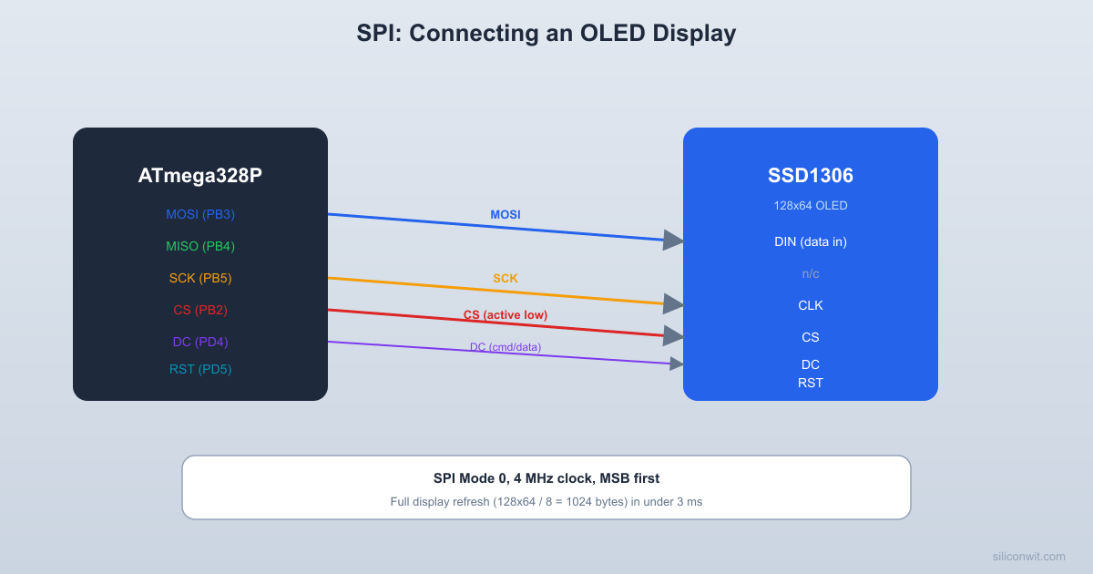
SPI Protocol Fundamentals
SPI uses four signals: MOSI (Master Out Slave In), MISO (Master In Slave Out), SCK (Serial Clock), and SS (Slave Select, active low).
  SPI Master-Slave Connection:
  ATmega328P (Master)         SSD1306 OLED (Slave)  +------------------+       +-------------------+  |                  |       |                   |  |  MOSI (PB3) -----+------>| DIN (data in)     |  |                  |       |                   |  |  MISO (PB4) <----+-------| (not used)        |  |                  |       |                   |  |  SCK  (PB5) -----+------>| CLK (clock)       |  |                  |       |                   |  |  SS   (PB2) -----+------>| CS  (chip select) |  |                  |       |                   |  +------------------+       +-------------------+
  Data shifts out MOSI on each SCK edge.  SS must be LOW to select the slave.
The master generates the clock and drives MOSI while reading MISO. Data is exchanged simultaneously in both directions, one bit per clock edge. The slave is selected by pulling its SS line low. For a broader comparison of SPI, I2C, and other common bus topologies, see Digital Electronics: Bus Architecture and Interfaces.
Signal
ATmega328P Pin
Arduino Pin
Direction
MOSI
PB3
D11
Master to Slave
MISO
PB4
D12
Slave to Master
SCK
PB5
D13
Master output
SS
PB2
D10
Master output (active low)
Clock Polarity and Phase
SPI Mode
CPOL
CPHA
Clock Idle
Data Sampled On
0
0
0
Low
Rising edge
1
0
1
Low
Falling edge
2
1
0
High
Falling edge
3
1
1
High
Rising edge
The SSD1306 uses Mode 0 (CPOL=0, CPHA=0). Always check the peripheral datasheet to determine the correct mode.
SPI Register Configuration
The ATmega328P SPI peripheral is controlled by two registers. SPCR (SPI Control Register) enables the peripheral, sets master/slave mode, clock polarity/phase, and the prescaler. SPSR (SPI Status Register) contains the transfer-complete flag (SPIF) and an optional double-speed bit (SPI2X).
while (!(SPSR & (1<< SPIF))); /* Wait for transfer complete */
return SPDR;
}
SSD1306 OLED Wiring
The 7-pin SPI OLED module has the following connections:
OLED Pin
Function
Arduino Nano Pin
ATmega328P Pin
GND
Ground
GND
GND
VCC
Power (3.3V or 5V)
5V
VCC
D0 (CLK)
SPI Clock
D13
PB5 (SCK)
D1 (MOSI)
SPI Data
D11
PB3 (MOSI)
RES
Reset
D8
PB0
DC
Data/Command
D9
PB1
CS
Chip Select
D10
PB2 (SS)
SSD1306 Driver
The SSD1306 has a 128x64 pixel display organized into 8 pages. Each page is 8 pixels tall, and each byte in a page represents a vertical column of 8 pixels.
  SSD1306 display memory layout:
  128 columns  <------------------------------>  +-----+-----+-----+-- --+-----+ Page 0  |byte0|byte1|byte2| ...  |b127 | (rows 0-7)  +-----+-----+-----+-- --+-----+  +-----+-----+-----+-- --+-----+ Page 1  |b128 |b129 |b130 | ...  |b255 | (rows 8-15)  +-----+-----+-----+-- --+-----+   ...                             ...  +-----+-----+-----+-- --+-----+ Page 7  |b896 |b897 |b898 | ...  |b1023| (rows 56-63)  +-----+-----+-----+-- --+-----+
  Each byte = 8 vertical pixels:  bit 0 = top pixel, bit 7 = bottom  Total: 128 x 8 = 1024 bytes
The SSD1306 distinguishes between commands and data using the D/C pin: low for commands, high for pixel data. The initialization sequence configures the display for 128x64 resolution with horizontal addressing mode. After initialization, you write pixel data as a 1024-byte stream (128 columns by 8 pages, each page is 8 pixels tall).
The framebuffer is a 1024-byte array that mirrors the OLED memory layout: 128 columns by 8 pages. Each byte represents a vertical strip of 8 pixels with bit 0 at the top. To draw a character, you copy its bitmap data into the framebuffer at the correct column and page offset. After updating the buffer, flush the entire thing to the display in one SPI burst.
oled_cmd(0x21); oled_cmd(0); oled_cmd(127); /* Column range */
oled_cmd(0x22); oled_cmd(0); oled_cmd(7); /* Page range */
oled_data(framebuf, 1024);
}
Complete Firmware
#defineF_CPU16000000UL
#include<avr/io.h>
#include<avr/interrupt.h>
#include<util/delay.h>
#include<util/atomic.h>
/* Include all the SPI, OLED, and font code from above */
volatileuint32_t seconds =0;
ISR(TIMER1_COMPA_vect)
{
staticuint16_t subsec =0;
subsec++;
if (subsec >=1000) {
subsec =0;
seconds++;
}
}
staticvoidtimer1_init(void)
{
TCCR1A =0;
TCCR1B = (1<< WGM12) | (1<< CS11) | (1<< CS10);
OCR1A =249; /* 1 ms tick */
TIMSK1 = (1<< OCIE1A);
}
staticvoidformat_time(uint32_tsec, char*buf)
{
uint8_t h = (sec /3600) %24;
uint8_t m = (sec /60) %60;
uint8_t s = sec %60;
buf[0] ='0'+ h /10;
buf[1] ='0'+ h %10;
buf[2] =':';
buf[3] ='0'+ m /10;
buf[4] ='0'+ m %10;
buf[5] =':';
buf[6] ='0'+ s /10;
buf[7] ='0'+ s %10;
buf[8] ='\0';
}
intmain(void)
{
spi_init();
oled_init();
timer1_init();
sei();
uint32_t last_sec =0xFFFFFFFF;
while (1) {
uint32_t now;
ATOMIC_BLOCK(ATOMIC_RESTORESTATE) {
now = seconds;
}
if (now != last_sec) {
last_sec = now;
chartime_str[9];
format_time(now, time_str);
fb_clear();
fb_draw_string(30, 3, time_str); /* Centered on page 3 */
oled_flush();
}
}
}
SPI Clock Speed and Prescaler
The SPI transfer timing in Mode 0 (CPOL=0, CPHA=0) samples data on the rising edge of SCK. The SSD1306 uses this mode. The SPIF flag sets after 8 clocks, signaling the transfer is complete.
  SPI Mode 0 byte transfer:
  SCK:  _   _   _   _   _   _   _   _       | | | | | | | | | | | | | | | |  _____|  |_|  |_|  |_|  |_|  |_|  |_|__
  MOSI: X D7 X D6 X D5 X D4 X D3 X D2 X D1 X D0        (data changes on falling edge,         sampled on rising edge)
  CS:   ____                          ____            |________________________|
  SPIF: ______________________________                                      |__| set
The SPI clock speed is set by the SPI2X bit in SPSR and the SPR1/SPR0 bits in SPCR. The SSD1306 supports SPI clocks up to about 10 MHz, so the default F_CPU/4 (4 MHz) works well. If you need faster transfers, enable SPI2X for F_CPU/2 (8 MHz).
SPI2X
SPR1
SPR0
Clock Divider
Speed (16 MHz)
0
0
0
/4
4 MHz
0
0
1
/16
1 MHz
0
1
0
/64
250 kHz
0
1
1
/128
125 kHz
1
0
0
/2
8 MHz
1
0
1
/8
2 MHz
1
1
0
/32
500 kHz
1
1
1
/64
250 kHz
Exercises
Scale the font to 2x or 3x size for larger digits on the display. Multiply each bit in the font data to create bigger pixels.
Add a start/stop button: press to pause the clock, press again to resume. Show a “PAUSED” indicator on the display.
Implement a simple graphic: draw a horizontal progress bar that fills across the bottom of the screen each second, then resets.
Measure the time it takes to flush the entire framebuffer to the display. Calculate the theoretical minimum based on the SPI clock speed and 1024 bytes.
Summary
You now understand the SPI protocol at the register level: SPCR configuration, clock polarity and phase, master mode operation, and the transfer-complete flag. You wrote a complete SSD1306 OLED driver that handles initialization, command/data switching via the D/C pin, and framebuffer flushing. The real-time clock demonstrates how to combine SPI display output with timer-based timekeeping. SPI is the fastest on-chip serial bus and the foundation for interfacing with many embedded peripherals.
Comments