This final lesson takes a different approach. Instead of drawing schematics and placing components by hand, you will define the ATmega328P breakout board from Lesson 1 entirely in Python code. The circuit becomes a script you can version control, parameterize, and regenerate on demand. #KiCad #Python #SKiDL
Why Code-Based PCB Design?
Code Your Circuits
Every board you designed in Lessons 1 through 8 lives in binary KiCad project files. They work, but they are hard to diff, hard to parameterize, and impossible to generate programmatically. Code-based PCB design solves these problems:
Version control: a Python script diffs cleanly in Git, line by line. A binary .kicad_sch file does not.
Parametric designs: change one variable (crystal frequency, number of I/O pins, LED count) and regenerate the entire board.
Automation: generate 50 board variants from a single script with a loop.
Testing: write unit tests for your circuit definitions, catching wiring errors before you ever open KiCad.
Reproducibility: anyone can run your script and get the exact same netlist, every time.
Review: code review a circuit the same way you review firmware. Pull requests for hardware.
If you have taken the Code-Based Mechanical Design course, this is the electronics equivalent: replacing a GUI workflow with a script that produces the same output, but with all the benefits of code.
SKiDL + KiCad pcbnew Pipeline
──────────────────────────────────────────
circuit.py (SKiDL)
│
│ Define parts, connect nets
▼
generate_netlist()
│
▼
circuit.net (KiCad netlist)
│
▼
pcbnew Python API
│ Load netlist
│ Place components at (x, y)
│ Set board outline
▼
circuit.kicad_pcb
│
│ Route traces (interactive or
│ freerouter autorouter)
▼
Run DRC ──► Export Gerbers
Tools Overview
Two Python tools make code-based PCB design practical with KiCad:
SKiDL
A Python library for defining electronic circuits in code. You declare parts, connect pins to nets, and SKiDL generates a KiCad-compatible netlist. It replaces the schematic editor for circuit definition. Install with pip install skidl.
KiCad pcbnew API
KiCad’s built-in Python module for manipulating PCB files. It can load netlists, place components at specific coordinates, set board outlines, run DRC, and export manufacturing files. It replaces manual interaction with the PCB editor.
How they work together: SKiDL handles the “what” (which components, how they connect), while pcbnew handles the “where” (component placement, board outline, routing). SKiDL outputs a .net file that pcbnew imports, just as if you had drawn a schematic and exported a netlist through the GUI.
Setup
Install KiCad 9
You need KiCad installed for its symbol and footprint libraries. If you have been following this course, KiCad is already on your machine.
Run this script. If it prints the part details without errors, your environment is ready.
Building the ATmega328P Breakout in Code
This is the main event. You will recreate the entire Lesson 1 circuit (ATmega328P, crystal, voltage regulator, LEDs, ISP header, pin headers) as a Python script using SKiDL.
Power Supply Section
Start with the power input and 5V regulation, exactly matching Lesson 1’s barrel jack and AMS1117-5.0 circuit:
Each Part() call mirrors a component you placed in the Lesson 1 schematic. The += operator connects a pin to a net, replacing a wire in the schematic editor.
To use the circuit, combine all the sections above into a single file called atmega328p_breakout.py. The structure is straightforward: imports at the top, net declarations, then each subsection (power, MCU, crystal, reset, ISP, LEDs, headers), ending with ERC() and generate_netlist(). Run it with python atmega328p_breakout.py and SKiDL produces a .net file in the current directory that KiCad can import directly.
From Netlist to PCB
Once you have the netlist, you need to get it into a PCB layout. There are two paths: manual import through the KiCad GUI, or scripted placement using the pcbnew Python API.
Manual Import
Open KiCad and create a new project.
Open the PCB Editor (pcbnew).
File, Import Netlist and select the .net file generated by SKiDL.
Place components manually, just as you did in Lesson 1. All footprints, net connections, and reference designators come from the netlist.
Route traces, add copper pours, and run DRC as normal.
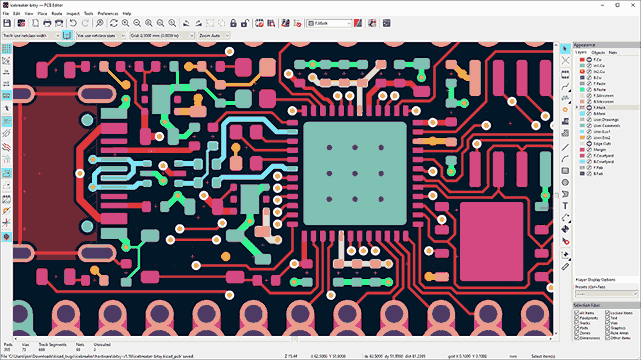
This is the simplest approach. You get the benefit of code-defined circuits with the familiar KiCad layout workflow.
Scripted Placement with pcbnew
For full automation, use KiCad’s pcbnew Python module to place components at specific coordinates:
"""
Basic pcbnew script to set up board outline and place components.
Run inside KiCad's scripting console or with the standalone pcbnew Python module.
print("Components placed. Open the board in KiCad to route traces.")
Parametric Design Example
The real power of code-based design is parameterization. Wrap the breakout circuit in a function that accepts parameters, and you can generate multiple board variants from one script. Here are the key parametric sections:
Three different board variants, three function calls. The breakout_minimal variant uses an 8 MHz crystal with different load capacitors, a single power LED, and only 8 I/O pins. The breakout_extended variant runs at 20 MHz with four LEDs. Each produces its own netlist file.
Automated DRC with Python
KiCad’s pcbnew module lets you run Design Rule Checks programmatically. This is useful in CI/CD pipelines or for batch-checking multiple board variants:
"""
Run DRC on a KiCad PCB file and report results.
Requires KiCad's pcbnew Python module.
"""
import pcbnew
defrun_drc(pcb_path):
"""Run DRC on a board file and return pass/fail with details."""
You can integrate this into a build script or GitHub Actions workflow. Every push to your repository triggers DRC, catching clearance violations and unconnected nets before you order boards.
KiCad Action Plugins
KiCad supports Python plugins that run inside the GUI, adding custom menu items and functionality. Here is a minimal plugin that stamps board information onto the silkscreen layer:
"""
KiCad Action Plugin: Add Board Info Text
Place this file in KiCad's scripting/plugins directory.
txt.SetPosition(pcbnew.FromMM(25,38)) # Near bottom center
txt.SetLayer(pcbnew.F_SilkS)
txt.SetTextSize(pcbnew.FromMM(1,1))
txt.SetTextThickness(pcbnew.FromMM(0.15))
board.Add(txt)
pcbnew.Refresh()
print(f"Added board info: {info_text}")
BoardInfoPlugin().register()
After placing the file in the plugins directory, restart KiCad. The plugin appears under Tools, External Plugins. One click adds a formatted label with the board name, revision, and date.
Limitations and the Road Ahead
Code-based PCB design is powerful but not a complete replacement for the GUI workflow. Here is an honest assessment:
What works well today:
Circuit definition and netlist generation (SKiDL is mature and reliable)
Parametric board variants from a single codebase
Automated DRC and manufacturing file export
Version control and code review for hardware designs
What is still maturing:
SKiDL generates netlists, not visual schematics. You lose the ability to glance at a schematic diagram for quick understanding. Some teams generate a schematic from the netlist after the fact for documentation.
Automated component placement works for simple boards but requires manual tuning for complex layouts.
Automated routing is not built into KiCad’s Python API. External tools like FreeRouting can help, but interactive routing in the GUI is still faster for most boards.
The pcbnew Python API changes between KiCad versions, so scripts may need updates when you upgrade.
The practical workflow:
The most effective approach combines both methods. Use Python and SKiDL for circuit definition (the “what”), then switch to KiCad’s GUI for layout refinement (the “where”). You get version control and parameterization for the circuit while keeping the visual, interactive layout tools where they matter most.
What You Have Learned
Course Summary: PCB Design with KiCad
Over nine lessons, you progressed from a beginner placing through-hole components to designing multi-layer mixed-signal boards and generating circuits from Python code:
Fundamentals (Lessons 1 and 2):
Schematic capture: symbols, wires, power flags, net labels, ERC
Comments