Breadboards are fine for prototyping, but loose jumper wires fall out, stray capacitance causes noise, and the whole setup falls apart when you move it. A custom PCB turns a fragile prototype into a solid, reproducible circuit you can hand to someone else and it just works. In this first lesson you will design a complete ATmega328P breakout board in KiCad 9 as a two-layer board so the same files can be sent to JLCPCB, milled on a CNC, or etched at home. The board is compact (66x53mm with rounded corners and four mounting holes), uses only through-hole components, and runs the same chip as an Arduino Uno, but built from scratch. The ATmega328P sits in a DIP socket, so once a chip is programmed on this board you can pop it out and drop it into any other circuit. The board doubles as a chip programmer for production builds. #KiCad #ATmega328P #PCBDesign
Schematic to PCB Workflow
──────────────────────────────────────────
1. Schematic 2. Netlist 3. PCB Layout
┌──────────┐ ┌──────────┐ ┌──────────┐
│ Place │ │ Export │ │ Import │
│ symbols, │───►│ netlist │───►│ footprts,│
│ wire nets│ │ (.net) │ │ route │
└──────────┘ └──────────┘ │ traces │
└────┬─────┘
4. DRC 5. Gerbers │
┌──────────┐ ┌──────────┐ │
│ Check │◄───│ Generate │◄────────┘
│ errors │ │ mfg files│
└──────────┘ └──────────┘
What We Are Building
ATmega328P Breakout Board
A minimal but complete microcontroller board: ATmega328P in DIP-28 package, 16 MHz crystal, ISP programming header, 5V power input with voltage regulator, power LED, user LED, reset button, decoupling capacitors, and pin headers exposing all I/O. Everything a standalone AVR project needs.
Board specifications:
Parameter
Value
MCU
ATmega328P-PU (DIP-28)
Clock
16 MHz crystal + 22 pF load capacitors
Power
7-12V via barrel jack J1 OR screw terminal J6 (both reverse-polarity protected through D3), regulated to 5V by LM7805. 5V direct input also possible via J4’s +5V and GND pins for users with regulated 5V supplies.
Programming
6-pin ISP header (USBasp or Arduino-as-ISP) and 6-pin FTDI header (USB-serial cable, after burning a bootloader)
Chip socket
28-pin DIP socket: program a chip on this board, pop it out, drop into any other circuit
I/O
2x 14-pin headers exposing all 20 usable GPIO plus AVCC, AREF, VIN, RESET, +5V, GND
LEDs
Power (green), User (red, on PB5/D13)
Size
66 x 53 mm with 3 mm rounded corners and 4 × M3 mounting holes, two-layer (F.Cu and B.Cu)
Components
All through-hole
Bill of Materials
Ref
Component
Package
Quantity
Notes
U1
ATmega328P-PU
DIP-28
1
The MCU itself
(socket)
28-pin DIP socket
DIP-28
1
Holds U1 so the chip can be swapped or transplanted
U2
LM7805
TO-220
1
5V linear regulator
D3
1N5817 Schottky diode
DO-41
1
Reverse-polarity protection on barrel jack input
Y1
16 MHz crystal
HC-49S
1
C1, C2
22pF ceramic
Through-hole
2
Crystal load capacitors
C3, C4
100nF ceramic
Through-hole
2
VCC and AVCC decoupling
C5
10uF electrolytic
Through-hole
1
Regulator input
C6
10uF electrolytic
Through-hole
1
Regulator output
C7
100nF ceramic
Through-hole
1
AREF filter cap
C8
100nF ceramic
Through-hole
1
FTDI auto-reset cap (DTR to RESET)
R1
10k
Through-hole
1
Reset pull-up
The board groups into seven subcircuits: power supply, MCU and clock, reset, ISP programming, FTDI programming, LEDs, and I/O breakout. Each schematic-capture section below opens with a small ASCII diagram showing the topology, then walks through the steps to build it in KiCad.
Run the installer and keep all default options. The standard library will be installed automatically.
Verify the installation by opening KiCad. You should see the project manager with options for Schematic Editor, PCB Editor, and other tools.
Project Setup
Open KiCad 9 and click File > New Project.
Name the project atmega328p-breakout and choose a location. KiCad creates a .kicad_pro project file, a .kicad_sch schematic file, and a .kicad_pcb board file.
Open the Schematic Editor by double-clicking the .kicad_sch file in the project tree.
KiCad Navigation Essentials
KiCad is keyboard-driven. These hotkeys work in both editors unless noted.
Navigation and selection
Action
How
Pan
Hold middle mouse button and drag (or right-click and drag)
Press L. Use for dense schematics or local connections.
Add global label (text in a box)
Press Ctrl+L. Preferred for prominent named nets like VIN, RESET, MOSI.
Add hierarchical label (arrow shape)
Press H. Only for multi-sheet hierarchical designs; skip on single-sheet.
Add no-connect flag (for unused MCU pins)
Press Q, click the pin
Editing components
Action
How
Move (wires break off)
Hover, press M, click to drop
Drag (wires stretch and stay attached)
Hover, press G, click to drop
Delete a wire segment
Click the wire, press Delete
Rotate
Hover, press R
Mirror
Hover, press X (horizontal) or Y (vertical)
Delete
Hover or select, press Delete
Edit value (e.g. 10uF, 330)
Hover, press V, type the new value, Enter
Edit reference (e.g. C2 to C5)
Hover over the reference text, double-click, type, Enter. Or use full properties (E)
Edit all properties (reference, value, footprint)
Hover, press E
Auto-number all references
Instead of manually renaming C? and R? placeholders or fixing C2 to C5 by hand, run Tools > Annotate Schematic once you have placed all the parts. KiCad numbers everything in the order it appears on the sheet, so C1, C2, C3... end up sensibly placed. You can re-run Annotate any time you add or remove components. This is faster than editing references one by one.
PCB editor specifics
Most actions in the PCB editor are reachable from the Place, Route, Edit, and Inspect menus, with shortcut keys as faster equivalents once you know them. Lead with the menu when in doubt: it works regardless of toolbar customization or icon visibility. The most common pairings:
Action
Menu
Shortcut
Start interactive router
Route > Route Single Track
X
Place a via mid-route
Route > Place Via
V
Add a copper pour zone
Place > Draw Filled Zones
Ctrl+Shift+Z
Fill all zones
Edit > Fill All Zones
B
Unfill all zones
Edit > Unfill All Zones
Ctrl+Shift+B
Edit a track’s width
(right-click the track > Properties)
E
Toggle lock on selection
(right-click > Lock)
L
Schematic Capture
The schematic defines what components are on the board and how they connect. We will build it section by section.
The power section takes 7-12V from the barrel jack, protects against reverse polarity, regulates to 5V, and provides decoupled power rails. We also expose the post-protection unregulated rail as VIN for breadboard use.
J1 (7-12V) D3 LM7805 (U2)
┌────────┐ ┌──────┐ ┌──────────┐
│ 1 Tip ●├─┤ ►| ├─┬── IN (1) ────┤1 3├── OUT (3) ──┬──── +5V
J6 alternate input (parallel with J1, also covered by D3):
┌────────┐
│ 1 + ●─├──► same node as J1 Tip (D3 anode)
│ 2 - ●─├──► same node as J1 Sleeve (GND)
└────────┘
Place the barrel jack. Press A (Add Symbol), search for Barrel_Jack_Switch, and place it on the left side of the sheet. The KiCad symbol numbers its pins:
Pin 1 = Tip (the inner contact, positive on center-positive wall warts)
Pin 2 = Sleeve (the outer contact, ground return)
Pin 3 = Switch contact (a built-in switch that breaks contact with pin 1 when a plug is inserted; useful for auto-disconnecting a battery, but we leave it unconnected here). Press Q and click on pin 3 to add a no-connect flag, otherwise ERC will report it as unconnected.
Place the reverse-polarity diode. Add D_Schottky (D3, 1N5817) in series with the barrel jack tip: anode to the jack tip, cathode to the rest of the input network. A diode only passes current from anode to cathode. With the wall wart correct, current flows forward through D3 and on to the regulator. If the wall wart is plugged in backwards, the diode is reverse-biased and blocks current entirely, sparing the regulator, the electrolytics, and the chip. Schottky diodes (like the 1N5817) are used here because their forward voltage drop is only about 0.3 V, so the regulator still sees enough headroom.
Place the voltage regulator. Add LM7805_TO220 (search for 7805 in the symbol library). Place it to the right of the barrel jack.
Place capacitors. Add two C_Polarized symbols for C5 (10uF, regulator input) and C6 (10uF, regulator output). Place C5 between the diode cathode and regulator input, C6 between the regulator output and the MCU power pins.
Add power port symbols. Press P (Add Power Port) and place +5V and GND symbols. Connect +5V to the regulator output and GND to the ground rail.
Label the unregulated rail as VIN. KiCad does not ship a VIN power port. Instead, draw the wire from the diode cathode to the regulator input pin, then press Ctrl+L (Add Global Label) and type VIN. Drop the boxed label onto the same wire. Anywhere else you want to tap this rail (the J4 pin, for example), just place another VIN global label on a wire and KiCad will treat them as the same net. (A plain net label L would also work; the boxed global form is preferred for prominent named nets so they stand out on the schematic.)
Add an alternate power input (J6). Some users will not have a barrel-jack adapter on hand. Add a 2-pin screw terminal in parallel with J1 so they can wire 7-12V directly. Press A, search Screw_Terminal_01x02 (or Conn_01x02 as a fallback), place it as J6 near J1. Wire J6 pin 1 to the same node as the barrel jack Tip (the wire feeding D3 anode), and J6 pin 2 to GND. Both inputs share D3 for reverse-polarity protection, so you can’t accidentally fry the board through J6 either.
Wire everything. Press W to draw wires. Connect:
Barrel jack Tip and J6 pin 1 to D3 anode (same node)
D3 cathode to C5 positive to the regulator input pin, with a VIN net label on this wire
Regulator output to C6 positive to the +5V net
Barrel jack Sleeve, J6 pin 2, C5 negative, regulator GND pin, C6 negative all to GND
MCU and Crystal
The MCU section has three small subcircuits: the 16 MHz crystal with two load caps, decoupling caps for VCC and AVCC, and an AREF filter cap.
XTAL1 ──┬── ┌────────┐ ──┬── XTAL2
│ │ Y1 │ │
│ │ 16MHz │ │
│ └────────┘ │
─┴─ ─┴─
C1 ─┬─ 22pF C2 ─┬─ 22pF
│ │
GND GND
       +5V                       +5V        │                         │        ├── VCC (pin 7)           ├── AVCC (pin 20)        │                         │       ─┴─                       ─┴─    C3 ─┬─ 100nF              C4 ─┬─ 100nF        │                         │       GND                       GND
   AREF (MCU pin 21) ──┬──                      ─┴─                   C7 ─┬─ 100nF                       │                      GND
All +5V symbols are the same net and all GND symbols are the same net; KiCad merges power ports by name. Drawing each cap on its own per-pin stack documents that C3 belongs next to pin 7 and C4 next to pin 20, so the PCB layout places them with short traces to their respective MCU pins.
Note: the VCC (pin 7) and AVCC (pin 20) text in the diagram above are pin-name annotations telling you which MCU pin the wire connects to. Do not add them as KiCad net labels. The chip’s symbol already shows VCC and AVCC inside its body (those are the pin labels), and the +5V power port already names the wire’s net. Adding extra VCC or AVCC labels triggers a multiple_net_names warning in ERC.
Place the ATmega328P. In KiCad’s symbol library, search for ATmega328P-P. The -P suffix indicates the PDIP-28 (through-hole) package. Place it in the center of the sheet. (Microchip’s full order code is ATmega328P-PU where the U means tube packaging, but KiCad’s symbol drops the order-code suffix.)
Connect power pins. Wire VCC (pin 7) and AVCC (pin 20) to +5V. Wire the visible GND pin (pin 8) to GND. The chip’s other GND pin (pin 22) is hidden in KiCad’s symbol but auto-connects to the GND net by name, so the netlist and PCB will both have it grounded. To see it for yourself, toggle View > Show Hidden Pins. Pin 22 then appears faintly near pin 8 in the symbol’s body.
Place decoupling capacitors. Add two C symbols (100nF each). Place C3 near VCC and C4 near AVCC. Connect each between the power pin and GND. These are critical for stable MCU operation.
Place the crystal. Add Crystal and place it near XTAL1 (pin 9) and XTAL2 (pin 10). Connect the crystal pins to XTAL1 and XTAL2.
Place crystal load capacitors. Add two C symbols (22pF each, C1 and C2). Connect one from XTAL1 to GND and one from XTAL2 to GND.
AREF pin. Add a C symbol (C7, 100nF) from AREF (pin 21) to GND. This decouples the analog reference voltage and improves ADC accuracy. The Arduino Uno schematic includes this cap by default, even on boards that don’t actively use the ADC.
Reset Circuit
R1 holds RESET high so the MCU runs normally. SW1 shorts RESET to GND when pressed, restarting the chip.
+5V
│
┌┴┐
R1 │ │ 10k
└┬┘
├──► RESET (MCU pin 1, ISP pin 5)
┌┴┐
SW1 │•│ (push to short)
└┬┘
│
GND
Place the pull-up resistor. Add R (10k, R1). Connect one end to the RESET pin (pin 1) and the other to +5V. This keeps the MCU running; pulling RESET low resets it.
Place the reset button. Add SW_Push. Connect one side to RESET and the other to GND. Pressing the button pulls RESET low.
Label the RESET net. Press Ctrl+L (Add Global Label), type RESET, and drop the boxed label on the wire connecting R1, MCU pin 1, and SW1. The same RESET label will be reused later on the ISP header (J2 pin 5) and the FTDI auto-reset cap (C8) so all four touchpoints merge into one net without crossing wires.
ISP Programming Header
The 6-pin ISP header lets you program the ATmega328P using a USBasp programmer or an Arduino acting as ISP. Use this header for fuses, the bootloader, or raw flash access.
J2 (AVR ISP, 2x3)
┌────┐
MISO ┤1 2├ VCC
SCK ┤3 4├ MOSI
RESET ┤5 6├ GND
└────┘
Place a 2x3 connector. Add AVR-ISP-6 from the Connector library. This symbol comes with the proper AVR ISP pin labels (MISO, VCC, SCK, MOSI, RESET, GND) already in place. If you can’t find it, Conn_02x03_Odd_Even works as a generic 2x3 fallback, but you have to label the pins yourself.
Wire the ISP signals:
Pin 1 (MISO) to PB4 (pin 18)
Pin 2 (VCC) to +5V (power port)
Pin 3 (SCK) to PB5 (pin 19)
Pin 4 (MOSI) to PB3 (pin 17)
Pin 5 (RESET): drop a RESET global label (Ctrl+L) on this pin’s wire so it merges with the RESET net you already labeled in the Reset Circuit section
Pin 6 (GND) to GND (power port)
FTDI Programming Header
The 6-pin FTDI header lets you program the ATmega328P from a regular USB-to-serial cable (FTDI, CP2102, or CH340 USB-to-UART). This requires a bootloader to be flashed first via ISP, after which uploads work the same way an Arduino Uno does. The DTR line on the cable pulses RESET through a 100nF cap so the bootloader catches the upload window automatically.
J5 (FTDI cable)
┌─────────────┐
│ 1 GND ├─────────────► GND
│ 2 CTS ├─────────────► GND
│ 3 VCC ├─────────────► +5V
│ 4 TXD ├─────────────► PD0/RXD (pin 2)
│ 5 RXD ├─────────────► PD1/TXD (pin 3)
│ 6 DTR ├──┤├──────────► RESET (pin 1)
└─────────────┘ C8
100nF
Place a 1x6 connector. Add Conn_01x06_Pin for J5. The pinout matches the FTDI Basic / FT232RL cable convention.
Place the auto-reset cap. Add a C symbol (C8, 100nF) connected between J5 pin 6 (DTR) and the RESET net. This passes only the DTR transition, not a steady DC level.
Wire the FTDI signals:
Pin 1 (GND) to GND (power port)
Pin 2 (CTS) tie to GND. The bootloader doesn’t use hardware flow control, but some FTDI cables leave CTS floating on their side and won’t send data unless CTS is grounded somewhere. Grounding it on the board guarantees uploads work with any cable. (This is what Arduino Pro Mini and SparkFun FTDI Basic do.)
Pin 3 (VCC) to +5V (power port)
Pin 4 (TXD, output from cable) to PD0/RXD (pin 2)
Pin 5 (RXD, input to cable) to PD1/TXD (pin 3)
Pin 6 (DTR) through C8 to a RESET global label (the same label name as in the Reset Circuit), which merges with the RESET net automatically
LEDs
The power LED is a permanent indicator that the +5V rail is alive. The user LED is on PB5, the same pin the Arduino IDE drives as D13, so any “blink” sketch lights it up.
   Power LED                       User LED on PB5 (Arduino D13, also ISP SCK)
       +5V                       PB5        │                         │       ┌┴┐                       ┌┴┐    R2 │ │ 330                R3 │ │ 330       └┬┘                       └┬┘       ┌┴┐                       ┌┴┐    D1 │▼│ (green)            D2 │▼│ (red)       └┬┘                       └┬┘        │                         │       GND                       GND
Power LED. Add LED (D1) and R (R2, 330). Connect +5V to R2, R2 to D1 anode, D1 cathode to GND.
User LED. Add LED (D2) and R (R3, 330). Connect PB5 (pin 19) to R3, R3 to D2 anode, D2 cathode to GND. PB5 is the classic Arduino D13 pin and is also ISP SCK on J2 pin 3. The same wire serves both purposes: the LED flickers visibly during ISP uploads as SCK clocks bytes into the chip, which is normal and identical to the behavior of the Arduino Uno’s onboard LED.
I/O Pin Headers
J3 (port D + low PB) J4 (port C + utility)
┌────────────┐ ┌────────────┐
│ 1 PD0 │ │ 1 PC0 │
│ 2 PD1 │ │ 2 PC1 │
│ 3 PD2 │ │ 3 PC2 │
│ 4 PD3 │ │ 4 PC3 │
│ 5 PD4 │ │ 5 PC4 │
│ 6 PD5 │ │ 6 PC5 │
│ 7 PD6 │ │ 7 AREF │
│ 8 PD7 │ │ 8 +5V(AVCC)│
│ 9 PB0 │ │ 9 RESET │
│10 PB1 │ │10 VIN │
│11 PB2 │ │11 +5V │
│12 PB3 │ │12 GND │
│13 PB4 │ │13 +5V │
│14 PB5 │ │14 GND │
└────────────┘ └────────────┘
Place two 1x14 connectors. Add Conn_01x14_Pin for J3 and J4. Place them on the left and right edges of the schematic. (The schematic symbol is generic; the footprint we assign later is the female socket variant so jumper wires plug directly into the finished board.)
Wire J3 to the port D and lower port B pins: PD0-PD7 (pins 2-6, 11-13) and PB0-PB5 (pins 14-19). That is 14 pins, all I/O.
Wire J4 to the port C pins plus utility lines: PC0-PC5 (pins 23-28), AREF, RESET, VIN, then three +5V pins and two GND pins for breadboard power distribution. That fills all 14 positions and gives easy access to every power rail and the reset line. (AVCC is the chip’s analog supply pin and is wired directly to +5V in this design, so the header carries +5V rather than a separately filtered AVCC rail.)
PB6 (XTAL1, pin 9) and PB7 (XTAL2, pin 10) are not exposed because the crystal needs them. PC6 (pin 1) is RESET and is exposed via J4 as the reset line. Together J3 and J4 break out all 20 usable GPIO plus every power rail.
Schematic Polish
A working schematic and a readable schematic are different things. The reviewer of your circuit (your future self included) reads it to understand intent, so make it easy to follow.
Group functional sections with labeled boxes. Use Place > Draw Text Box to drop a labeled rectangle around each subcircuit in one step: type the heading (“Power Supply”, “MCU and Clock”, etc.) into the dialog, click OK, then click two corners to size the box. The text-box frames and labels are graphical only, they have no electrical effect, they just guide the eye:
Power Supply (J1, D3, U2, C5, C6)
MCU and Clock (U1, Y1, C1-C4, C7)
Reset (R1, SW1)
ISP Programming (J2)
FTDI Programming (J5, C8)
LEDs (R2, R3, D1, D2)
I/O Breakout (J3, J4)
Edit the title block. Open File > Page Settings. The title block lives at the bottom right of every sheet and is the first thing a reviewer reads. Fill in at least:
Field
Example
Title
ATmega328P Breakout Board
Date
2026-04-30
Revision
A
Company
Your name or organization
Comment 1
Through-hole, two-layer (F.Cu and B.Cu)
Comment 2
Programming: ISP (J2) and FTDI (J5)
The Revision field is the one most often overlooked. Bump it (A to B, or 1.0 to 1.1) every time you change the schematic and re-export manufacturing files. It keeps you from confusing yourself when you have several iterations on the bench.
Logo (optional). Use Place > Draw Image to drop a PNG of your logo on the sheet. To put a logo in the title block of every sheet you create, edit the page-layout worksheet template instead (File > Page Settings > Page Layout File). Worksheet editing is its own small skill; skip it for now and just place the image manually if you want a logo on this sheet.
Final ERC pass. After polish, re-run Inspect > Electrical Rules Check. Graphical shapes and text never break electrical connectivity, but it is worth verifying that nothing was nudged off a pin while you were arranging things.
Assign Component Values
Before leaving the schematic editor, assign values to every component:
Double-click each component to open its properties.
Set the Value field:
C1, C2: 22pF
C3, C4, C7, C8: 100nF
C5, C6: 10uF
R1: 10k
R2, R3: 330
Y1: 16MHz
D3: 1N5817
Pre-ERC checklist. Before running ERC, verify these common issues:
PWR_FLAG on each externally-supplied power net. Search PWR_FLAG in the symbol library and place one on VIN and one on GND. The flag tells ERC “this net is fed from outside the schematic.” Without flags, ERC reports power_pin_not_driven errors on the LM7805 input and on the GND rail. Do not place PWR_FLAG on +5V: the LM7805 output pin is already a “Power output” type and drives that net, so adding a flag triggers a pin_to_pin “two power outputs connected” error.
No-connect flags on intentionally-unused pins. Press Q and click any pin you do not plan to wire (J1 pin 3 was the obvious one earlier). Without flags, ERC reports pin_not_connected errors.
Global labels must appear at least twice. If you used a global label like RXD, TXD, PB3, PC0, etc. at one end of a connection, the same label must also exist at the other end so KiCad can merge them. A single dangling label triggers a global_label_dangling warning.
Label casing matters.PC0 and pc0 are different nets in KiCad. Use one casing convention (uppercase is conventional) and stick to it.
Run Inspect > Electrical Rules Check (ERC). The dialog opens; click Run ERC to start the check. Fix any remaining errors and warnings. The ERC should pass with zero errors before you proceed.
Assign Footprints
Every schematic symbol needs a physical footprint for the PCB.
Open Tools > Assign Footprints (or click the footprint assignment icon in the toolbar) and assign each symbol its physical footprint.
The table below is a curated shortcut for this lesson. In a real workflow, you would let KiCad narrow the choices down for you: select a symbol, then enable the Filter by symbol toggle on the footprint list. Most KiCad symbols carry a ki_fp_filters hint (the chip’s package code, like DIP*W7.62mm* or TO?220*), so the right side shrinks from thousands of footprints down to a handful that match the part’s package. You pick from that short list. For SMD parts you would also cross-check against the recommended land pattern in the part’s datasheet.
Experienced users frequently draw their own custom footprints in KiCad’s Footprint Editor when no library footprint matches: unusual mechanical parts, custom-molded connectors, parts with non-standard pin pitches, or new components without a matching library entry. The workflow is to read the manufacturer’s recommended land pattern from the datasheet and translate the dimensions into KiCad pads and outlines. For this lesson every part has a stock library footprint, so you do not need to draw any.
Symbol
Footprint
ATmega328P-P
Package_DIP:DIP-28_W7.62mm (use a DIP-28 socket, same footprint)
TerminalBlock_Phoenix:TerminalBlock_Phoenix_MKDS-1,5-2-5.08_1x02_P5.08mm_Horizontal (5.08mm pitch, ships with a 3D model so the 3D viewer renders it correctly). The generic TerminalBlock:TerminalBlock_MaiXu_MX126-5.0-02P_1x02_P5.00mm works as a fallback but has no 3D model.
Click Apply, Save Schematic & Continue, then close the footprint assignment dialog.
PCB Layout
Now we translate the schematic into a physical board.
Import Netlist
In the Schematic Editor, run Tools > Update PCB from Schematic (or press F8). A dialog opens listing every component, footprint, and net change. Click Update PCB, then Close. The PCB Editor opens with all components imported along with their connections (the netlist).
All components appear stacked in one corner. Click to place them roughly in the center of the board.
Define Board Outline
A board shape is part of the design statement. Arduino’s boards have rounded corners and obvious mounting holes for a reason: they look intentional, fit into enclosures, and survive being handled. We follow the same approach with a 66 mm wide × 53 mm tall outline, giving the chip and headers comfortable breathing room.
Target shape: 66 × 53 mm rectangle, 3 mm rounded corners, 4 × M3 mounting holes ~6 mm in from each edge.
←────────────────────────── 66 mm ───────────────────────────→
Select the Edge.Cuts layer in the Layers panel on the right (it should turn yellow / become active).
Draw a rectangle for the outline. Use Place > Draw Rectangle. Click the bottom-left corner at (0, 0), then the top-right corner at (66, 53). You can type each corner exactly using the X/Y coordinate fields at the bottom of the editor, or set your grid to 1 mm and snap to it.
Fillet the corners. Right-click anywhere on the rectangle, choose Shape Modifications > Fillet Lines, and set the radius to 3 mm. KiCad converts each sharp corner into a smooth 3 mm arc in one shot. This is much faster than drawing separate lines and arcs by hand.
After filleting, the outline is a closed rounded rectangle on Edge.Cuts.
Add four M3 mounting holes. Open Place > Add Footprint (or press A), search for MountingHole_3.2mm_M3. Place one near each corner, about 6 mm in from each edge so there is roughly 4.4 mm of board material around each hole:
bottom-left: (6, 6)
bottom-right: (60, 6)
top-left: (6, 47)
top-right: (60, 47)
These positions sit clear of the J3 and J4 footprints and clear of the rounded-corner radius.
Optional: add silkscreen labels. Use Place > Draw Text on the F.SilkS layer to mark the board name, version, or your initials near the bottom-right. This survives etching and looks professional.
The four mounting holes anchor the board to standoffs or an enclosure with M3 screws. Their 6 mm inset from each edge is the sweet spot: close enough to the corners to keep the board square under load, far enough that the surrounding board material won’t crack when the screw is tightened.
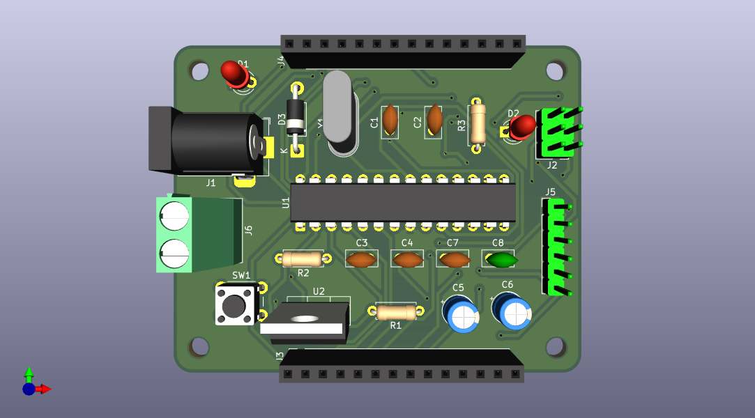
Component Placement
Good placement is the most important step in PCB layout. Place components logically before routing any traces.
Pin headers (J3, J4) define the I/O edges: J4 along the top, J3 along the bottom. Female sockets at 2.54mm pitch let you plug jumper wires directly into the board to reach sensors, modules, or a breadboard. (If you prefer the board to plug into a breadboard like a chip, use male PinHeader_1x14_P2.54mm_Vertical footprints instead, with the two rows 15.24mm apart for standard breadboard rails.)
ATmega328P (U1) in its DIP-28 socket, centered between J3 and J4. Orient it so pin 1 is at the top-left.
Barrel jack (J1) on the upper-left edge, oriented so the plug inserts from outside the board.
Screw terminal (J6) directly below J1 on the left edge so wires can be inserted easily. J1 and J6 share the same input node.
Reverse-polarity diode (D3) along the top, between J1 and the crystal area, on the path from the input node toward the regulator.
Voltage regulator (U2) at the bottom-left, with C5 and C6 (input and output bulk caps) at the bottom-right on the same power rail.
Crystal and load caps (Y1, C1, C2) centered above U1. Keep the traces down to XTAL1 and XTAL2 short to minimize noise pickup.
Decoupling caps (C3, C4, C7) in a row below U1, with the shortest possible traces up to VCC, AVCC, and AREF.
ISP header (J2) at the top-right, accessible from the board edge for easy programmer connection.
FTDI header (J5) on the right edge, with C8 (the auto-reset cap) placed in the bottom cap row on the way from DTR back to RESET.
Reset button (SW1) on the left-middle, below J6 and within thumb reach of the board edge.
LEDs and limiter resistors: D1 (power, GREEN) at the top-left corner with R2 (330) in the bottom row; D2 (user, RED) with R3 (330) at the top-mid-right; R1 (10k pull-up) in the bottom row alongside the decoupling caps.
Design Rules
Before routing, set up design rules that work for any of the three manufacturing paths (fab, CNC, or home etch):
Open File > Board Setup… in the PCB Editor (or click the board-with-gear icon on the top toolbar). In the dialog, expand Design Rules in the left tree and click Net Classes.
Set the Default net class. You will see several columns, only the first four matter for this board:
Clearance:0.3 mm (12 mil), the minimum gap between any two copper features. Generous enough for home etching, well within fab limits.
Track Width:0.5 mm (about 20 mil), comfortable for hand routing
Via Size:0.8 mm, the outer pad diameter
Via Hole:0.4 mm, the drill diameter inside the via pad
Vias are how a trace jumps between F.Cu (top) and B.Cu (bottom). On this board most layer transitions land on through-hole component pads, which act as natural vias once the lead is soldered on both sides. Standalone vias are only needed for trace transitions that don’t sit on a component pad.
Leave the remaining columns at their defaults: Microvia Size and Microvia Hole are for HDI boards (laser-drilled vias), and DP Width / DP Gap are for differential pairs (USB, Ethernet). Neither applies here. PCB Color is cosmetic and only affects the 3D viewer.
Add a Power net class for +5V and GND:
Clearance:0.3 mm
Track Width:0.8 mm, wider so it carries the regulator current without dropping voltage
Click OK to save the rules.
The Constraints page (under Design Rules in the same dialog) sets the absolute floor values DRC will flag, separately from the per-class working values above. Leave it at defaults for this board: our 0.5 mm tracks and 0.3 mm clearance are well above any sensible minimum, so nothing in Constraints will ever trigger. You only revisit it when ordering from a fab whose minimums you want DRC to enforce (e.g. JLCPCB’s 0.127 mm trace/clearance limits).
Routing
Layer strategy. Use B.Cu (bottom copper) as the primary signal layer and F.Cu (top copper) as the jumper layer for crossings. Components mount on the top side with leads passing through to the bottom, where most soldering happens. Through-hole pads connect both copper layers wherever a lead is soldered, so layer transitions on a component pad are free; standalone vias are only needed for transitions in the middle of a trace.
Route power first on B.Cu. In the Layers panel on the right, click B.Cu so it is the active layer (the row turns highlighted). Open Route > Route Single Track (or press X) to start routing, then click pad-to-pad. Connect all +5V, VIN, and GND traces first using the wider Power net class.
Route the crystal. Keep XTAL1 and XTAL2 traces short and parallel on B.Cu, directly under the chip pads, away from other signals. This is the most noise-sensitive part of the circuit, do not let other signals run between or under it.
Route ISP signals. MISO, MOSI, SCK, and RESET from the MCU to the ISP header. Keep them reasonably short.
Route FTDI signals. RX (PD1) and TX (PD0) to J5, plus the DTR-through-C8-to-RESET path.
Route remaining signals. Connect the LEDs, reset button, and pin headers. The interactive router (Route > Route Single Track, or X, then click pads) will push existing traces out of the way.
Handle crossings with a via. When the next segment would have to cross an existing track, jump to the other layer instead. The transition is a via, “free” if it lands on a through-hole component pad and otherwise inserted as a standalone via. Aim for as few standalone vias as you can manage, two or three is normal for this board.
The mid-route flow:
Route on B.Cu (blue), click click click toward the destination pad
You see the next segment would cross an existing track
Press V, then left-click to place the via at the cursor
The router now lays the next track on F.Cu (preview is red instead of blue) so it can pass over the obstacle
Left-click on the destination pad to finish
Your active layer in the Layers panel stays on B.Cu the whole time, you don’t need to switch it back. The via just sends the current segment to F.Cu temporarily; the next route you start will begin on B.Cu again automatically.
Ctrl+Z undoes the last segment if you misclick. Press ~ (tilde) on a pad to highlight every pad on that net, useful when you’re unsure which pads still need to be connected.
Add ground pours on both layers. In the Layers panel on the right, click F.Cu to make it active. Open Place > Draw Filled Zones (or press Ctrl+Shift+Z, or click the cross-hatched-square icon on the right toolbar) to start a zone. Click the first corner of the board outline, the Copper Zone Properties dialog appears, set Net to GND, leave the other defaults, click OK. Click the remaining three corners of the board outline, then double-click to close the polygon. Open Edit > Fill All Zones (or press B) to fill. Repeat the same steps with B.Cu active. Pours on both sides shorten ground return paths, improve noise immunity, and (for home etching) reduce the amount of copper that has to be dissolved away.
If you want to draw the zones now but route a few more tracks before filling, skip the fill step. The zone outlines stay empty until you fill them later. To unfill at any point use Edit > Unfill All Zones (or Ctrl+Shift+B).
Run DRC. Open Inspect > Design Rules Check and click Run DRC. Fix any errors. Common issues:
Unconnected pads (missed a trace)
Clearance violations (traces too close together)
Unrouted nets (the ratsnest lines still showing)
The DRC should pass with zero errors and zero unconnected items.
3D Preview
Before manufacturing, check the 3D view:
Open View > 3D Viewer (or press Alt+3).
Visually inspect:
Are all components on the correct side?
Does the barrel jack orient correctly?
Do the pin headers align for breadboard use?
Is there enough clearance between tall components?
Rotate the view to check from all angles. This catches placement mistakes that are invisible in the 2D view.
Manufacturing
A finished KiCad design can travel three different paths to a working board. Pick the one that fits your tools, budget, and timeline. The same project files work for all three.
Path
Cost
Lead time
Tools needed
Order from a fab (JLCPCB, OSHPark, PCBWay)
~2-10 USD for 5 boards
1-2 weeks shipping
None
CNC mill the board yourself
One-time machine cost
~1 hour per board
CNC mill with isolation routing
Home etch (toner transfer)
A few cents per board
~2 hours per board
Laser printer, ferric chloride, drill
All three paths start from the same exported files. The next section covers what to export; pick a manufacturing subsection after that.
Generate Manufacturing Files
Export Gerbers (for fab houses and most CNC software). Go to File > Plot. Select these layers: F.Cu, B.Cu, F.SilkS, B.SilkS, F.Mask, B.Mask, Edge.Cuts. Set output format to Gerber. Leave Mirrored unchecked. Click Plot. KiCad writes one .gbr file per layer to the project’s gerbers/ folder.
Generate the drill file. Still in the Plot dialog, click Generate Drill Files. Select Excellon format and PTH and NPTH in single file. Click Generate Drill File. This tells the fab (or your drill press) where to make holes.
(Fab path only) Zip the Gerbers and drill file. Most fab houses want a single .zip containing all the .gbr and .drl files. Select them in your file manager and create the archive.
(Home etch path only) Export copper layers as PDF as well. Re-open File > Plot, switch output format to PDF, select F.Cu and B.Cu. Check Mirrored for the F.Cu plot (because the printed sheet gets flipped face-down onto the copper, so the design must be pre-mirrored to land right-reading). Leave B.Cu unmirrored. Click Plot. CNC software reads Gerbers directly and handles side flipping internally, so PDFs are not needed for milling.
Path A: Order from JLCPCB (or any fab house)
The fastest, cheapest, and least error-prone path. JLCPCB charges around 2 USD for five 2-layer boards plus shipping.
Go to jlcpcb.com, click Order Now, and upload the zipped Gerbers from the previous step.
Confirm the auto-detected settings: Layers: 2, Dimensions: 66 x 53 mm, PCB Color: Green (or whichever you prefer), Surface Finish: HASL (cheapest, fine for hand soldering). Leave everything else at defaults.
Place the order. Boards typically arrive in 1-2 weeks depending on shipping option.
When the boards arrive, jump straight to the Soldering and Assembly section below.
The plated through-holes connect F.Cu to B.Cu automatically wherever there is a pad or via, so no manual wire-vias are needed. This is the recommended path for a first project.
Path B: CNC Milling
Mills cut isolation channels around traces instead of removing copper chemically. No chemicals, full control, but you need a CNC machine with sub-millimeter precision.
Convert the Gerbers to G-code with a tool like FlatCAM or pcb2gcode. Generate one G-code file for F.Cu, one for B.Cu, and one for the drill file. Use a 0.2 mm or 0.3 mm V-bit for isolation routing.
Mount a double-sided copper-clad board to the mill bed. Drill two alignment holes outside the board outline first (e.g., 3 mm holes through both the copper and the bed waste board). These let you flip the board and mill the second side in registration with the first.
Mill B.Cu first with the board copper-side up. Then drill the component holes through both layers.
Flip the board over (re-pinning into the alignment holes), and mill F.Cu.
Manual wire-vias. For any standalone via that did not land on a through-hole component pad, push a short bare-copper wire through the via hole and solder it on both sides. Trim flush. Through-hole component leads themselves do not need this since the lead handles both sides when soldered.
Cut the board to the rounded outline with the mill or a small saw, then sand the edges smooth.
Path C: Home Etching (Toner Transfer)
The classic DIY route. Cheap and accessible with kitchen tools, but the most labor-intensive of the three.
Print the copper layers. Print F.Cu (mirrored) and B.Cu (unmirrored) on glossy magazine paper or dedicated toner transfer paper using a laser printer. Inkjets do not work; the toner is what transfers to the copper.
Prepare a double-sided copper-clad board. Cut it to about 72 x 60 mm (slightly larger than the 66 × 53 board outline so you have margin for handling). Clean both copper surfaces with fine sandpaper (400-600 grit) and isopropyl alcohol. The surfaces must be spotless for the toner to stick.
Transfer the top layer. Place the F.Cu printout face-down on one side of the copper. Iron over it with a clothes iron set to maximum heat (no steam) for about 5 minutes, applying firm, even pressure. Let it cool, then soak in warm water and gently peel the paper away. The toner stays on the copper.
Drill alignment holes. Drill the four M3 mounting holes through the board now (using the drill file as a reference). These holes register the second side to the first.
Transfer the bottom layer. Flip the board, line up the B.Cu printout with the alignment holes (poke the printout onto two pins through two of the M3 holes), and iron it on the same way.
Etch the board. Submerge the board in ferric chloride solution (available at electronics stores). Agitate gently, both sides get etched at once. The exposed copper dissolves in 10-30 minutes depending on temperature and concentration. The areas protected by toner remain as traces.
Clean the board. Remove the board when all exposed copper is gone. Rinse with water. Remove the remaining toner with acetone or fine sandpaper.
Drill the remaining holes. Use a 0.8 mm drill bit for component leads and a 1.0 mm bit for pin headers and the barrel jack. A drill press or hand drill with a PCB drill bit works. Drill straight down so both copper layers stay aligned around each hole.
Add manual wire-vias. Without electroplating, F.Cu and B.Cu are not yet electrically connected at via holes. For each standalone via (and any through-hole component pad that needs a connection on a side that won’t have a soldered lead), push a short bare-copper wire through the hole and solder it on both sides. Trim flush. Through-hole component leads handle this automatically once they are soldered top and bottom.
Trim the board to the rounded outline using a coping saw or rotary tool, then sand the edges smooth.
Inspect. Check for:
Broken traces (fix with a thin wire and solder)
Short circuits between traces (scrape away with a craft knife)
Clean, properly-sized holes
Wire-vias soldered on both sides
Soldering and Assembly
Install the DIP socket first. Solder the 28-pin DIP socket for U1. This lets you remove the ATmega328P without desoldering. Align the notch with pin 1.
Solder low-profile components next. Resistors (R1, R2, R3), ceramic capacitors (C1-C4, C7, C8), the crystal (Y1), and the Schottky diode (D3, watch the cathode stripe orientation).
Then taller components. Electrolytic capacitors (C5, C6, watch polarity), LEDs (D1, D2, longer leg is anode/positive), the reset button (SW1).
Connectors last. Barrel jack (J1), screw terminal (J6), ISP header (J2), FTDI header (J5), pin headers (J3, J4). These are the tallest components.
Voltage regulator. Solder U2 (LM7805) on top. Attach a small clip-on heatsink if you plan to run from 12V at higher current.
Insert the ATmega328P into the DIP socket. Match pin 1 (marked with a dot on the chip) with the socket notch.
First Power-On
Visual inspection. Before applying power, check every solder joint under magnification. Look for solder bridges (shorts between adjacent pins) and cold joints (dull, lumpy solder).
Continuity check. Use a multimeter in continuity mode. Verify:
No short between +5V and GND
+5V reaches VCC (pin 7) and AVCC (pin 20)
GND reaches pins 8 and 22
Apply power. Connect a 9V battery or 7-12V power supply to the barrel jack. The power LED (D1) should light up.
Measure voltages. With the multimeter, verify:
5.0V (±0.1V) between +5V and GND
5.0V at ATmega328P VCC (pin 7)
If the voltage is wrong, power off immediately and check the regulator connections.
Firmware: Blink LED
We will program the ATmega328P directly over ISP, without the Arduino IDE or bootloader. This proves the board works at the hardware level.
Add C:\msys64\mingw64\bin to your system PATH so avr-gcc and avrdude work from any terminal.
Older guides point to WinAVR. That project was last released in 2010, ships only as a portable build that is awkward to put on PATH, and is no longer maintained. Avoid it unless you have a specific reason.
Blink Code
Save this as blink.c:
/*
* blink.c - Toggle LED on PB5 (pin 19) every 500ms
* ATmega328P @ 16 MHz, no Arduino, no bootloader
*/
#defineF_CPU16000000UL
#include<avr/io.h>
#include<util/delay.h>
intmain(void) {
DDRB |= (1<< PB5); /* Set PB5 as output */
while (1) {
PORTB ^= (1<< PB5); /* Toggle PB5 */
_delay_ms(500);
}
}
Compile and Flash
Connect a USBasp programmer (or Arduino-as-ISP) to the 6-pin ISP header. The ribbon cable pin 1 should match the header pin 1.
If you are using an Arduino Uno as an ISP programmer, replace -c usbasp with -c arduino -P /dev/ttyACM0 -b 19200 (adjust the port for your system).
The red user LED (D2) should now blink at 1 Hz (500ms on, 500ms off). If it does, your board is fully functional: power supply, crystal, MCU, and I/O all work.
Optional: Burn a Bootloader for FTDI Uploads
The ISP path above writes raw firmware directly into flash. For day-to-day work it is faster to use the FTDI header instead, which lets you upload sketches over a USB-serial cable without an ISP programmer attached. This requires a small program called a bootloader to be written into the upper 512 bytes of flash. Once the bootloader is there, every reset (including the auto-reset triggered by the FTDI cable’s DTR line) gives the bootloader a brief window to receive new firmware over the UART before the main program runs.
You burn the bootloader once, with the ISP programmer:
After this, you can disconnect the ISP programmer and upload sketches from any tool that speaks the Arduino bootloader protocol (the Arduino IDE, PlatformIO, or avrdude -c arduino):
The FTDI cable’s DTR line pulses RESET through C8 each time you start an upload, so the bootloader is always ready. This is how every Arduino Uno on the planet is programmed.
The two programming paths coexist on the same board:
ISP via J2 for fuses, bootloader, full flash erase, or recovering a chip with a corrupted bootloader.
FTDI via J5 for fast everyday uploads.
What You Have Learned
Lesson 1 Complete
KiCad skills:
Created a new project, built a complete schematic, assigned footprints
Designed a two-layer PCB layout with design rules, ground pours on both sides, and DRC
Exported manufacturing files (Gerbers for fab, copper PDFs for CNC and home etch, drill file)
Linear voltage regulation with input/output capacitors
Reverse-polarity protection with a Schottky diode
DTR auto-reset for serial bootloader uploads
Component placement strategy for noise immunity
Manufacturing skills:
Three paths from KiCad to a working board: fab order, CNC milling, home etching
Manual wire-via technique for connecting F.Cu and B.Cu without electroplating
Drilling, alignment, and inspection
Through-hole soldering order (low to high components), with both sides soldered to bridge the layers
Firmware skills:
Bare-metal AVR C programming (no Arduino abstraction)
AVR fuse configuration for external crystal
ISP programming with avrdude
Bootloader burning and serial uploads via FTDI cable
Reusable workflow: because the chip lives in a DIP socket, this board doubles as a chip programmer. Flash a fresh ATmega328P here, pop it out, and drop it into any standalone application circuit. The board pays for itself many times over.
Comments