Choose SPI When
You need high speed (displays, external Flash, high-speed ADCs), you have pins to spare for CS lines, and you want full-duplex communication. SPI is the fastest standard serial bus.
Microcontrollers communicate with sensors, displays, memory chips, and other MCUs through serial buses. SPI, I2C, and UART are the three protocols you will use most often in embedded programming. This lesson takes you below the HAL function calls to the actual signal waveforms on the wires, so that when something goes wrong (and it will), you can look at a logic analyzer capture and diagnose the problem. #SPI #I2C #UART
A parallel bus sends multiple bits simultaneously, one per wire. The internal buses inside your MCU (AHB, APB) are parallel: 32 data lines carry a full word in one clock cycle.
Advantages: Fast (high throughput per clock cycle).
Disadvantages: Many wires, crosstalk at high frequencies, difficult to route on PCBs, expensive connectors.
A serial bus sends bits one at a time over fewer wires. SPI, I2C, and UART are all serial.
Advantages: Few wires (2 to 4), simple PCB routing, long-distance capable.
Disadvantages: Lower throughput per clock cycle (but high clock rates compensate).
| Property | Parallel (32-bit AHB) | SPI | I2C | UART |
|---|---|---|---|---|
| Data wires | 32 | 1 (+ 1 return) | 1 (bidirectional) | 1 TX + 1 RX |
| Clock wire | 1 (shared) | 1 | 1 | None (asynchronous) |
| Additional wires | Address, control | CS (one per slave) | None | None |
| Typical speed | 72 MHz (internal) | 1-50 MHz | 100-400 kHz (up to 3.4 MHz) | 9600-115200 baud (up to ~1 Mbaud) |
| Topology | Point-to-point | Master + multiple slaves | Multi-master, multi-slave | Point-to-point |
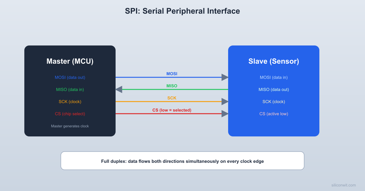
SPI uses four signals (three for unidirectional communication):
| Signal | Name | Direction | Function |
|---|---|---|---|
| SCLK | Serial Clock | Master to slave | Clock signal generated by the master |
| MOSI | Master Out Slave In | Master to slave | Data from master to slave |
| MISO | Master In Slave Out | Slave to master | Data from slave to master |
| CS/SS | Chip Select | Master to slave | Active-low, selects which slave is active |
SPI is essentially two shift registers connected in a ring:
Master Slave ┌──────────┐ ┌──────────┐ │ Shift │──── MOSI ──────→│ Shift │ │ Register │ │ Register │ │ (8-bit) │←─── MISO ──────│ (8-bit) │ └──────────┘ └──────────┘ │ │ └──────── SCLK ──────────────→│ │ │ └──────── CS ────────────────→│On each clock edge, one bit shifts out of the master’s shift register (on MOSI) and one bit shifts in from the slave (on MISO). After 8 clock cycles, the master and slave have exchanged one byte.
This is exactly the 74HC595 shift register from Lesson 4, but now the shift register has both an input and an output, forming a bidirectional data exchange.
SPI has four modes defined by two parameters:
| Mode | CPOL | CPHA | Clock Idle | Data Captured On | Data Changed On |
|---|---|---|---|---|---|
| 0 | 0 | 0 | Low | Rising edge | Falling edge |
| 1 | 0 | 1 | Low | Falling edge | Rising edge |
| 2 | 1 | 0 | High | Falling edge | Rising edge |
| 3 | 1 | 1 | High | Rising edge | Falling edge |
Mode 0 is the most common. Many sensors and displays default to Mode 0.
CS:    ─────┐                                          ┌─────            └──────────────────────────────────────────┘
SCLK:  ─────┐  ┌──┐  ┌──┐  ┌──┐  ┌──┐  ┌──┐  ┌──┐  ┌──┐  ┌─            └──┘  └──┘  └──┘  └──┘  └──┘  └──┘  └──┘  └──┘
MOSI:  ═══╡ D7 ╞╡ D6 ╞╡ D5 ╞╡ D4 ╞╡ D3 ╞╡ D2 ╞╡ D1 ╞╡ D0 ╞═══
MISO: ═══╡ D7 ╞╡ D6 ╞╡ D5 ╞╡ D4 ╞╡ D3 ╞╡ D2 ╞╡ D1 ╞╡ D0 ╞═══Each slave needs its own CS line. The master pulls one CS low to communicate with that slave while keeping all others high (deselected).
Master ┌──────┐ SCLK ─┤ ├─── CS0 ──→ Slave 0 MOSI ─┤ ├─── CS1 ──→ Slave 1 MISO ─┤ ├─── CS2 ──→ Slave 2 └──────┘This means SPI requires one additional MCU pin per slave device. With many slaves, you can use a decoder (Lesson 3) to generate CS signals from a smaller number of address pins.
I2C uses only two wires for any number of devices:
| Signal | Name | Function |
|---|---|---|
| SCL | Serial Clock | Clock signal (driven by master) |
| SDA | Serial Data | Bidirectional data line (shared) |
Both lines use open-drain drivers with external pull-up resistors (typically 4.7K ohm to VCC). Any device can pull the line low, but no device drives it high. The pull-up resistor pulls the line high when no device is pulling it low.
  I2C bus topology
       VCC          VCC        │            │       [4.7K]       [4.7K]        │            │  ──────┼────────────┼──────── SCL  ──────┼────────────┼──────── SDA        │            │  ┌─────┴──┐   ┌────┴───┐  │ Master │   │BME280  │  │ (MCU)  │   │ 0x76   │  └────────┘   └────────┘        │            │  ┌─────┴──┐   ┌────┴───┐  │SSD1306 │   │DS3231  │  │ 0x3C   │   │ 0x68   │  └────────┘   └────────┘
All devices share two wires. Pull-ups required on both lines.Each slave device on the bus has a unique 7-bit address (some devices use 10-bit addressing). The master sends the address at the start of each transaction, and only the addressed slave responds.
Common I2C addresses:
| Device | Typical Address |
|---|---|
| BME280 sensor | 0x76 or 0x77 |
| SSD1306 OLED | 0x3C or 0x3D |
| DS3231 RTC | 0x68 |
| EEPROM (24C256) | 0x50-0x57 |
A complete I2C write transaction to send one data byte:
SDA: ─┐ ┌───┬───┬───┬───┬───┬───┬───┬───┬───┬───┬───┬───┬───┬───┬───┬───┬───┬─┐ ┌── └─┤A6 │A5 │A4 │A3 │A2 │A1 │A0 │R/W│ACK│D7 │D6 │D5 │D4 │D3 │D2 │D1 │D0 │ACK├─┘ └───┴───┴───┴───┴───┴───┴───┴───┴───┴───┴───┴───┴───┴───┴───┴───┴───┴───┘ START 7-bit address W Ack 8-bit data Ack STOP (from master) (0) (slave) (from master) (slave)A unique feature of I2C: the slave can hold SCL low to pause the transfer if it needs more time to process data. The master must wait for SCL to go high before continuing. This is called clock stretching and is why SCL must be open-drain (the slave needs to pull it low).
| Mode | Maximum Clock |
|---|---|
| Standard | 100 kHz |
| Fast | 400 kHz |
| Fast-Plus | 1 MHz |
| High-Speed | 3.4 MHz |
Most embedded projects use Standard (100 kHz) or Fast (400 kHz) mode.
UART uses two data lines with no clock:
| Signal | Direction | Function |
|---|---|---|
| TX | Transmitter to receiver | Data output |
| RX | Receiver to transmitter | Data input |
| GND | Common | Shared ground reference |
Since there is no clock, both sides must agree on the data rate (baud rate) beforehand. This is why UART is “asynchronous.”
  UART point-to-point wiring
  Device A              Device B  ┌────────┐            ┌────────┐  │     TX ├───────────→│ RX     │  │        │            │        │  │     RX │◄───────────┤ TX     │  │        │            │        │  │    GND ├────────────┤ GND    │  └────────┘            └────────┘
TX of one device connects to RX of the other (crossover wiring). Shared ground is required.A standard UART frame consists of:
Idle ─────┐ ┌───┬───┬───┬───┬───┬───┬───┬───┬───┬─────── Idle └───┤D0 │D1 │D2 │D3 │D4 │D5 │D6 │D7 │(P)├─────── Start 8 data bits (LSB first) Parity Stop bit (opt.) bit(s)| Component | Bits | Function |
|---|---|---|
| Start bit | 1 | Always 0 (low). Signals the beginning of a frame. |
| Data bits | 5-9 (usually 8) | The actual data, sent LSB first. |
| Parity bit | 0-1 | Optional error detection (even or odd parity). |
| Stop bit(s) | 1-2 | Always 1 (high). Signals the end of the frame. |
The baud rate specifies how many bits per second are transmitted. Common rates:
| Baud Rate | Bit Period | Byte Period (8N1) |
|---|---|---|
| 9600 | 104.2 us | 1.04 ms |
| 115200 | 8.68 us | 86.8 us |
| 921600 | 1.09 us | 10.9 us |
“8N1” means 8 data bits, No parity, 1 stop bit (the most common configuration). Each byte takes 10 bit periods (1 start + 8 data + 1 stop).
Without a clock, the receiver uses the start bit to synchronize:
For this to work reliably, the transmitter and receiver baud rates must match within about 2-3%. If the rates drift too far apart, bit sampling falls at the wrong time and data corrupts.
| Standard | Voltage Levels | Connector |
|---|---|---|
| TTL UART | 0V (low) and 3.3V or 5V (high) | Pin headers |
| RS-232 | -12V (high) and +12V (low) | DB-9 connector |
| RS-485 | Differential pair | Screw terminals |
MCU UART pins operate at TTL levels (3.3V or 5V). To connect to a PC serial port (RS-232), you need a level converter like the MAX232. Most modern connections use a USB-to-TTL serial adapter (like the FTDI FT232 or CH340) that handles the conversion.
| Feature | SPI | I2C | UART |
|---|---|---|---|
| Wires | 3 + 1 per slave | 2 (shared) | 2 (point-to-point) |
| Clock | Yes (master) | Yes (master) | No (asynchronous) |
| Speed | Up to 50 MHz | Up to 3.4 MHz | Up to ~1 Mbaud |
| Duplex | Full duplex | Half duplex | Full duplex |
| Addressing | CS pin per slave | 7-bit address | None (point-to-point) |
| Acknowledgment | None (by default) | ACK/NACK per byte | None (or parity bit) |
| Typical use | Fast peripherals (display, Flash, ADC) | Sensors, RTCs, EEPROMs | Debug console, GPS, Bluetooth modules |
| Pin count for 4 slaves | 7 (SCLK, MOSI, MISO, 4xCS) | 2 (SCL, SDA) | 8 (4 TX + 4 RX pairs) |
Choose SPI When
You need high speed (displays, external Flash, high-speed ADCs), you have pins to spare for CS lines, and you want full-duplex communication. SPI is the fastest standard serial bus.
Choose I2C When
You have many low-speed devices (sensors, RTCs, EEPROMs) and want to minimize pin usage. Two wires connect to all devices on the bus regardless of count.
Choose UART When
You need a simple point-to-point connection with no clock synchronization, such as a debug serial console, GPS module, or Bluetooth module. UART is also the simplest protocol to debug with a logic analyzer.
A logic analyzer captures digital signals and displays them as timing diagrams. Inexpensive USB logic analyzers (Saleae clones or compatible) cost a few dollars and support protocol decoding for SPI, I2C, and UART.
Connect probes to the signal lines (SCLK, MOSI, MISO, CS for SPI; SCL, SDA for I2C; TX for UART). Always connect the analyzer’s GND to the circuit’s GND.
Set the sample rate to at least 4 times the bus clock frequency. For SPI at 1 MHz, sample at 4 MHz or higher.
Trigger on the CS falling edge (SPI), START condition (I2C), or TX falling edge (UART).
Capture a transaction and examine the waveform.
Enable protocol decoding in your analyzer software. It will overlay the decoded bytes on the waveform, showing addresses, data values, and ACK/NACK.
SPI problems:
I2C problems:
UART problems:
A master sends 0xA5 to a slave via SPI Mode 0, MSB first. Draw the sequence of bits on MOSI for all 8 clock cycles.
0xA5 = 10100101 in binary.
| Clock Cycle | SCLK Rising Edge | MOSI |
|---|---|---|
| 1 | First | 1 (bit 7) |
| 2 | Second | 0 (bit 6) |
| 3 | Third | 1 (bit 5) |
| 4 | Fourth | 0 (bit 4) |
| 5 | Fifth | 0 (bit 3) |
| 6 | Sixth | 1 (bit 2) |
| 7 | Seventh | 0 (bit 1) |
| 8 | Eighth | 1 (bit 0) |
Each bit is sampled on the rising edge and changed on the falling edge.
You want to write to a device at address 0x50. What is the full first byte sent on the bus (including the R/W bit) for a write operation? What about for a read?
The first byte is the 7-bit address shifted left by 1, with the R/W bit in bit 0.
Write: (0x50 << 1) | 0 = 0xA0 (binary: 10100000)
Read: (0x50 << 1) | 1 = 0xA1 (binary: 10100001)
In C:
uint8_t write_addr = (0x50 << 1); // 0xA0uint8_t read_addr = (0x50 << 1) | 1; // 0xA1At 115200 baud, how long does it take to transmit the string “Hello” (5 characters)? Assume 8N1 framing.
Each character requires 10 bits (1 start + 8 data + 1 stop).
5 characters = 50 bits.
Time per bit =
Total time =
HAL Functions Demystified
HAL_SPI_Transmit() generates SCLK pulses, shifts data out on MOSI, shifts data in on MISO, and manages CS. HAL_I2C_Master_Transmit() generates START, sends the address, checks ACK, sends data, and generates STOP. Now you know every step.
Debugging Communication
When a sensor does not respond, a logic analyzer shows you exactly what is on the wire. Is the address correct? Is the slave ACKing? Is the clock running? These are impossible to diagnose from code alone.
Bit-Banging
If your MCU does not have a hardware SPI or I2C peripheral on the pins you need, you can implement the protocol in software by toggling GPIO pins. This is called bit-banging. Understanding the signal-level protocol is essential for writing a correct bit-bang implementation.
Protocol Selection
Choosing between SPI, I2C, and UART for a project is a design decision that affects pin count, speed, PCB complexity, and software effort. Understanding each protocol at the signal level helps you make the right choice.
| Protocol | Signals | Clock | Speed | Best For |
|---|---|---|---|---|
| SPI | SCLK, MOSI, MISO, CS | Synchronous (master) | Up to 50 MHz | High-speed peripherals |
| I2C | SCL, SDA | Synchronous (master) | Up to 3.4 MHz | Multiple low-speed devices |
| UART | TX, RX | Asynchronous | Up to ~1 Mbaud | Point-to-point, debug console |
In the next lesson, you will explore ADC and DAC: how analog voltages are converted to digital numbers and back.
Comments