// Audio recorder using DMA ping-pong buffering with ADC and SPI flash storage
#include "hardware/dma.h"
#include "hardware/adc.h"
#include "hardware/spi.h"
#include "hardware/pwm.h"
#include "hardware/irq.h"
#include "hardware/gpio.h"
// -------------------------------------------------------
// -------------------------------------------------------
#define MIC_PIN 26 // ADC0 input (microphone)
#define BUTTON_PIN 10 // Record start/stop button
#define PWM_PIN 18 // PWM audio output
#define LED_PIN 25 // Onboard LED (recording indicator)
#define FLASH_MOSI_PIN 15
#define FLASH_MISO_PIN 12
// -------------------------------------------------------
// -------------------------------------------------------
#define BUF_SIZE 1024 // Samples per buffer
#define BUF_BYTES (BUF_SIZE * 2) // Bytes per buffer (16-bit samples)
// Flash storage parameters
#define FLASH_MAX_ADDR 0x400000 // 4 MB total
#define FLASH_SECTOR_SIZE 4096
#define FLASH_PAGE_SIZE 256
#define CMD_WRITE_ENABLE 0x06
#define CMD_PAGE_PROGRAM 0x02
#define CMD_READ_DATA 0x03
#define CMD_SECTOR_ERASE 0x20
#define CMD_READ_STATUS 0x05
#define CMD_CHIP_ERASE 0xC7
#define CMD_JEDEC_ID 0x9F
// -------------------------------------------------------
// -------------------------------------------------------
uint16_t buf_a[BUF_SIZE];
uint16_t buf_b[BUF_SIZE];
volatile int buffer_ready = -1; // -1 = none, 0 = A ready, 1 = B ready
volatile bool recording = false;
uint32_t flash_write_addr = 0;
uint32_t flash_read_addr = 0;
uint32_t recorded_length = 0; // Total bytes recorded
// -------------------------------------------------------
// -------------------------------------------------------
static inline void cs_select(void) {
gpio_put(FLASH_CS_PIN, 0);
static inline void cs_deselect(void) {
gpio_put(FLASH_CS_PIN, 1);
spi_init(FLASH_SPI, 10 * 1000 * 1000);
gpio_set_function(FLASH_SCK_PIN, GPIO_FUNC_SPI);
gpio_set_function(FLASH_MOSI_PIN, GPIO_FUNC_SPI);
gpio_set_function(FLASH_MISO_PIN, GPIO_FUNC_SPI);
gpio_set_dir(FLASH_CS_PIN, GPIO_OUT);
gpio_put(FLASH_CS_PIN, 1);
void flash_wait_done(void) {
uint8_t cmd = CMD_READ_STATUS;
spi_write_blocking(FLASH_SPI, &cmd, 1);
spi_read_blocking(FLASH_SPI, 0, &status, 1);
void flash_write_enable(void) {
uint8_t cmd = CMD_WRITE_ENABLE;
spi_write_blocking(FLASH_SPI, &cmd, 1);
void flash_sector_erase(uint32_t addr) {
spi_write_blocking(FLASH_SPI, cmd, 4);
void flash_page_program(uint32_t addr, const uint8_t *data, size_t len) {
if (len > FLASH_PAGE_SIZE) len = FLASH_PAGE_SIZE;
spi_write_blocking(FLASH_SPI, cmd, 4);
spi_write_blocking(FLASH_SPI, data, len);
void flash_read_data(uint32_t addr, uint8_t *data, size_t len) {
spi_write_blocking(FLASH_SPI, cmd, 4);
spi_read_blocking(FLASH_SPI, 0, data, len);
uint32_t flash_read_jedec_id(void) {
uint8_t cmd = CMD_JEDEC_ID;
spi_write_blocking(FLASH_SPI, &cmd, 1);
spi_read_blocking(FLASH_SPI, 0, id, 3);
return (id[0] << 16) | (id[1] << 8) | id[2];
// Write a full buffer (BUF_BYTES) to flash, handling sector erases and page boundaries
void flash_write_buffer(const uint8_t *data, size_t total_len) {
while (written < total_len) {
uint32_t addr = flash_write_addr + written;
// If we are at a sector boundary, erase the sector first
if ((addr % FLASH_SECTOR_SIZE) == 0) {
flash_sector_erase(addr);
// Calculate how many bytes we can write in this page
size_t page_offset = addr % FLASH_PAGE_SIZE;
size_t page_remaining = FLASH_PAGE_SIZE - page_offset;
size_t chunk = total_len - written;
if (chunk > page_remaining) chunk = page_remaining;
flash_page_program(addr, data + written, chunk);
flash_write_addr += total_len;
// -------------------------------------------------------
// -------------------------------------------------------
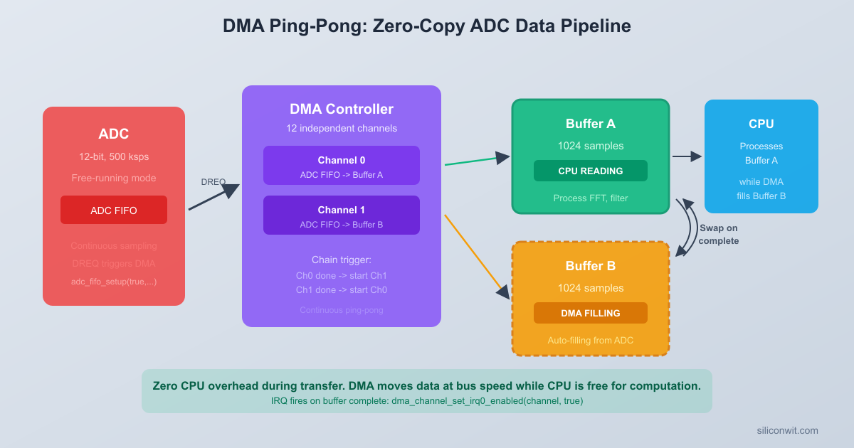
void dma_irq_handler(void) {
if (dma_hw->ints0 & (1u << dma_chan_a)) {
dma_hw->ints0 = 1u << dma_chan_a; // Clear interrupt flag
buffer_ready = 0; // Buffer A is full
if (dma_hw->ints0 & (1u << dma_chan_b)) {
dma_hw->ints0 = 1u << dma_chan_b; // Clear interrupt flag
buffer_ready = 1; // Buffer B is full
// -------------------------------------------------------
// -------------------------------------------------------
void adc_dma_init(void) {
adc_select_input(0); // ADC0 = GP26
// Set sample rate: 48 MHz / 96 = 500 kHz max rate
// For 8 kHz: divider = 500000 / 8000 - 1 = 61.5 (using adc_set_clkdiv which adds 1)
// More precisely: 48000000 / (96 * 8000) = 62.5, so clkdiv = 62.5 - 1 = 61.5
// But the SDK function expects the full divider value
float clkdiv = (48000000.0f / 8000.0f / 96.0f) - 1.0f;
1, // DREQ asserted when at least 1 sample in FIFO
false // Keep full 12-bit samples (no 8-bit shift)
// Claim two DMA channels
dma_chan_a = dma_claim_unused_channel(true);
dma_chan_b = dma_claim_unused_channel(true);
dma_channel_config cfg_a = dma_channel_get_default_config(dma_chan_a);
channel_config_set_transfer_data_size(&cfg_a, DMA_SIZE_16);
channel_config_set_read_increment(&cfg_a, false);
channel_config_set_write_increment(&cfg_a, true);
channel_config_set_dreq(&cfg_a, DREQ_ADC);
channel_config_set_chain_to(&cfg_a, dma_chan_b);
dma_channel_configure(dma_chan_a, &cfg_a,
BUF_SIZE, // Transfer count
dma_channel_config cfg_b = dma_channel_get_default_config(dma_chan_b);
channel_config_set_transfer_data_size(&cfg_b, DMA_SIZE_16);
channel_config_set_read_increment(&cfg_b, false);
channel_config_set_write_increment(&cfg_b, true);
channel_config_set_dreq(&cfg_b, DREQ_ADC);
channel_config_set_chain_to(&cfg_b, dma_chan_a);
dma_channel_configure(dma_chan_b, &cfg_b,
BUF_SIZE, // Transfer count
// Enable interrupts for both channels on IRQ0
dma_channel_set_irq0_enabled(dma_chan_a, true);
dma_channel_set_irq0_enabled(dma_chan_b, true);
irq_set_exclusive_handler(DMA_IRQ_0, dma_irq_handler);
irq_set_enabled(DMA_IRQ_0, true);
// -------------------------------------------------------
// -------------------------------------------------------
void start_recording(void) {
printf("Recording started...\n");
gpio_put(LED_PIN, 1); // LED on = recording
// Drain any leftover ADC FIFO entries
// Start Channel A, which will chain to B when done
dma_channel_start(dma_chan_a);
void stop_recording(void) {
// Abort both DMA channels
dma_channel_abort(dma_chan_a);
dma_channel_abort(dma_chan_b);
recorded_length = flash_write_addr;
gpio_put(LED_PIN, 0); // LED off
printf("Recording stopped. %u bytes stored.\n", (unsigned)recorded_length);
// -------------------------------------------------------
// -------------------------------------------------------
void pwm_audio_init(void) {
gpio_set_function(PWM_PIN, GPIO_FUNC_PWM);
uint slice = pwm_gpio_to_slice_num(PWM_PIN);
uint channel = pwm_gpio_to_channel(PWM_PIN);
// Configure PWM for audio output
// Wrap at 4095 to match 12-bit ADC range
pwm_set_wrap(slice, 4095);
pwm_set_chan_level(slice, channel, 0);
pwm_set_enabled(slice, true);
void play_recording(void) {
if (recorded_length == 0) {
printf("No recording to play.\n");
printf("Playing back %u bytes...\n", (unsigned)recorded_length);
uint slice = pwm_gpio_to_slice_num(PWM_PIN);
uint channel = pwm_gpio_to_channel(PWM_PIN);
uint8_t page_buf[FLASH_PAGE_SIZE];
while (addr < recorded_length) {
size_t chunk = recorded_length - addr;
if (chunk > FLASH_PAGE_SIZE) chunk = FLASH_PAGE_SIZE;
flash_read_data(addr, page_buf, chunk);
// Output samples via PWM
for (size_t i = 0; i + 1 < chunk; i += 2) {
uint16_t sample = page_buf[i] | (page_buf[i + 1] << 8);
sample &= 0x0FFF; // Mask to 12 bits
pwm_set_chan_level(slice, channel, sample);
// Wait for one sample period (125 us at 8 kHz)
// Silence output after playback
pwm_set_chan_level(slice, channel, 0);
printf("Playback complete.\n");
// -------------------------------------------------------
// -------------------------------------------------------
gpio_set_dir(BUTTON_PIN, GPIO_IN);
gpio_pull_up(BUTTON_PIN);
bool button_pressed(void) {
static bool last_state = true; // Pull-up: idle = high
static uint32_t debounce_time = 0;
bool current = gpio_get(BUTTON_PIN);
if (current != last_state) {
if (time_us_32() - debounce_time > 200000) { // 200 ms debounce
debounce_time = time_us_32();
if (!current) { // Button pressed (active low)
// -------------------------------------------------------
// -------------------------------------------------------
sleep_ms(2000); // Wait for USB serial to connect
printf("=== RP2040 Audio Sampler ===\n");
gpio_set_dir(LED_PIN, GPIO_OUT);
// Initialize peripherals
uint32_t jedec_id = flash_read_jedec_id();
printf("Flash JEDEC ID: 0x%06X\n", jedec_id);
if ((jedec_id & 0xFF0000) == 0) {
printf("WARNING: Flash not detected. Check wiring.\n");
printf("Press button to start/stop recording.\n");
printf("Press and hold for 2s to play back.\n");
uint32_t press_start = 0;
press_start = time_us_32();
// Detect long press for playback (button held > 1.5 seconds)
if (!gpio_get(BUTTON_PIN) && press_start != 0 && !held) {
if (time_us_32() - press_start > 1500000) {
// Short press toggles recording
if (gpio_get(BUTTON_PIN) && press_start != 0 && !held) {
if (time_us_32() - press_start > 50000) { // Debounce
// Process completed DMA buffers during recording
if (recording && buffer_ready >= 0) {
int buf_idx = buffer_ready;
// Check if we have space in flash
if (flash_write_addr + BUF_BYTES > FLASH_MAX_ADDR) {
// Write the completed buffer to flash
flash_write_buffer(data, BUF_BYTES);
Comments