Variable Placement
When you declare const uint8_t table[] = {1,2,3};, the compiler places it in Flash (saving SRAM). Without const, it goes in SRAM. On a tiny MCU with 2 KB SRAM, this distinction matters enormously.
Your microcontroller has several types of memory, and understanding them changes how you write firmware. Declaring a const array puts it in Flash (no RAM used). A global variable lives in SRAM. Writing calibration data to EEPROM keeps it safe across power cycles. This lesson explains how each memory technology stores bits, how the bus system connects the CPU to memory, and how the memory map gives every byte a unique address. #Memory #SRAM #Flash
All digital memory falls into two categories:
| Category | Retains Data Without Power? | Speed | Examples |
|---|---|---|---|
| Volatile | No | Fast | SRAM, DRAM |
| Non-volatile | Yes | Slower | Flash, EEPROM, ROM |
Microcontrollers typically contain:
Some MCUs (like the ESP32) use external SPI Flash. Others (like the STM32F103) have all three on-chip.
Each bit in SRAM is stored by a circuit called a 6T cell. It consists of two cross-coupled inverters that form a bistable latch (similar to the SR latch from Lesson 4), plus two access transistors controlled by a word line.
Conceptual structure:
Word Line │ ┌───────┼───────┐ │ │ │ Access Cross-coupled Access FET Inverter Pair FET │ │ │ └───┬───┘ ┌───┘ │ │ Bit Line Bit Line (complement)The two inverters hold the cell in one of two stable states: storing a 0 or storing a 1. The access transistors connect the cell to the bit lines when the word line is activated (during a read or write).
Key properties of SRAM:
| Property | Value |
|---|---|
| Read speed | 1 clock cycle (typically) |
| Write speed | 1 clock cycle |
| Endurance | Unlimited read/write cycles |
| Data retention | Only while powered |
| Cell size | 6 transistors per bit (relatively large) |
| Power | Consumes power continuously to maintain state |
When you write:
int x = 42;The compiler allocates space in SRAM for x. The CPU can read and write this location in a single clock cycle, which is essential for performance. Variables, the stack (function calls, local variables, return addresses), and the heap (dynamic allocation) all live in SRAM.
| MCU | SRAM Size |
|---|---|
| ATmega328P | 2 KB |
| STM32F103C8T6 (Blue Pill) | 20 KB |
| ESP32 | 520 KB |
| RP2040 (Pico) | 264 KB |
With only 2 KB on an ATmega328P, every byte counts. Understanding that each variable consumes SRAM helps you write memory-efficient firmware.
Flash memory stores bits using a special transistor with a floating gate: an electrically isolated conductor surrounded by insulating oxide layers.
How it works:
Programmed (storing 0): Electrons are forced onto the floating gate by applying a high voltage (around 10-20V internally). The trapped electrons raise the transistor’s threshold voltage, making it harder to turn on.
Erased (storing 1): The electrons are removed from the floating gate by applying a voltage in the opposite direction. The threshold voltage returns to its normal level.
Reading: A normal read voltage is applied to the control gate. If the cell is erased (threshold normal), the transistor conducts and the bit reads as 1. If programmed (threshold high), the transistor does not conduct and the bit reads as 0.
Key properties of Flash:
| Property | Value |
|---|---|
| Read speed | Fast (comparable to SRAM in many MCUs) |
| Write speed | Slow (microseconds to milliseconds per page) |
| Erase granularity | Page or sector (cannot erase single bytes) |
| Endurance | 10,000 to 100,000 erase/write cycles |
| Data retention | 10 to 20 years (specified by manufacturer) |
| Property | NOR Flash | NAND Flash |
|---|---|---|
| Read access | Random (byte-addressable) | Sequential (page-based) |
| Read speed | Fast | Moderate |
| Write speed | Slow | Moderate |
| Erase block size | 64-256 KB | 16-512 KB |
| Cost per bit | Higher | Lower |
| Used for | MCU program memory | USB drives, SD cards, SSDs |
Most microcontrollers use NOR Flash for internal program storage because it allows the CPU to execute code directly from Flash (execute-in-place, or XIP). The STM32F103 has 64 KB of NOR Flash where your compiled firmware lives.
Flash has two important constraints:
Cannot write individual bytes. Flash is organized into pages (typically 1-4 KB on MCUs). To change any byte in a page, you must erase the entire page first, then write the new data.
Erase sets all bits to 1. Programming can only change bits from 1 to 0. To change a 0 back to 1, you must erase the entire page.
This is why firmware updates take time: the bootloader must erase each Flash page before writing new firmware.
| MCU | Flash Size |
|---|---|
| ATmega328P | 32 KB |
| STM32F103C8T6 (Blue Pill) | 64 KB |
| ESP32 | 4 MB (external SPI Flash) |
| RP2040 (Pico) | 2 MB (external QSPI Flash) |
EEPROM uses the same floating-gate technology as Flash but with one critical difference: EEPROM can erase and write individual bytes, while Flash must erase entire pages.
This byte-level granularity makes EEPROM ideal for storing small amounts of configuration data that change infrequently: calibration values, device IDs, user settings.
Key properties of EEPROM:
| Property | Value |
|---|---|
| Read speed | Fast |
| Write speed | Slow (3-5 ms per byte, typically) |
| Erase granularity | Single byte |
| Endurance | 100,000 to 1,000,000 write cycles |
| Data retention | 20+ years |
| MCU | Internal EEPROM |
|---|---|
| ATmega328P | 1 KB |
| STM32F103 | None (emulated in Flash) |
| ESP32 | None (emulated in Flash) |
| External I2C EEPROM (24C256) | 32 KB |
The STM32F103 does not have dedicated EEPROM. Instead, ST provides an “EEPROM emulation” library that uses two Flash pages to simulate byte-level writes. This technique uses page rotation: when one page fills up, modified data is copied to the other page, and the original page is erased.
With 100,000 write cycles per cell, writing to the same EEPROM address in a tight loop can wear it out in minutes. Wear leveling distributes writes across multiple addresses to extend the total lifespan.
// BAD: writes to the same address every loop iterationwhile (1) {    eeprom_write(0x00, sensor_value);  // Will wear out address 0x00    delay_ms(10);}
// BETTER: rotate through multiple addressesuint16_t write_index = 0;while (1) {    eeprom_write(write_index, sensor_value);    write_index = (write_index + 1) % EEPROM_SIZE;    delay_ms(10);}
Address bus, data bus, and control signals
┌───────┐ ┌────────┐ │ │══ Address [31:0] ════→│ │ │ CPU │ │ Memory │ │ │◄═ Data [31:0] ══════►│ or │ │ │ │Periph. │ │ │── RD / WR ──────────→│ │ │ │── Chip Select ───────→│ │ └───────┘ └────────┘ 32 address lines: select location 32 data lines: carry read/write data Control lines: read, write, enableThe CPU communicates with memory (and peripherals) through buses: groups of parallel signal lines that carry addresses, data, and control signals.
| Bus | Function | Width (STM32F103) |
|---|---|---|
| Address bus | Specifies which memory location to access | 32 bits (4 GB addressable) |
| Data bus | Carries the data being read or written | 32 bits |
| Control bus | Read/write signal, clock, chip select | Several individual signals |
When the CPU executes x = *((volatile uint32_t *)0x40021000);:
0x40021000 on the address bus.x (in SRAM).This entire process typically completes in one or two clock cycles for SRAM and Flash, but may take more cycles for slower peripherals (adding “wait states”).
When the CPU executes *((volatile uint32_t *)0x40021000) = 0x00000001;:
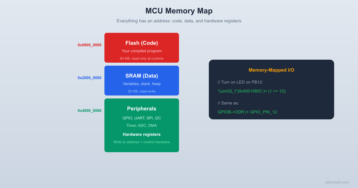
0x40021000 on the address bus.0x00000001 on the data bus.A memory map defines how the entire address space is divided among different types of memory and peripherals. Every address in the 32-bit address space (0x00000000 to 0xFFFFFFFF) is assigned to a specific resource.
  MCU Memory Map (STM32F103)
0xFFFFFFFF ┌──────────────────────┐ │ Cortex-M3 internals │ 0xE0000000 ├──────────────────────┤ │ (reserved) │ 0x40024000 ├──────────────────────┤ │ Peripherals (AHB) │ 0x40000000 ├──────────────────────┤ │ (reserved) │ 0x20005000 ├──────────────────────┤ │ SRAM (20 KB) │ │ variables, stack │ 0x20000000 ├──────────────────────┤ │ (reserved) │ 0x08010000 ├──────────────────────┤ │ Flash (64 KB) │ │ program code, const │ 0x08000000 └──────────────────────┘| Address Range | Size | Device |
|---|---|---|
| 0x00000000 - 0x0000FFFF | 64 KB | Flash (program code) |
| 0x08000000 - 0x0800FFFF | 64 KB | Flash (aliased) |
| 0x20000000 - 0x20004FFF | 20 KB | SRAM (variables, stack) |
| 0x40000000 - 0x40023FFF | varies | Peripheral registers (APB1, APB2, AHB) |
| 0xE0000000 - 0xE00FFFFF | varies | Cortex-M3 system peripherals (NVIC, SysTick, SCB) |
In the STM32 (and most modern MCUs), peripheral registers are mapped into the same address space as memory. This means you access a GPIO pin the same way you access a variable in SRAM: by reading or writing an address.
// This writes to SRAM (a variable)uint32_t x = 42;
// This writes to a GPIO peripheral register (same syntax, different address)*((volatile uint32_t *)0x4001080C) = 0x0001;  // GPIOA output data register
The CPU does not know or care whether the address points to SRAM, Flash, or a peripheral. It puts the address on the bus, and the decoder routes it to the right device. This unification is what makes memory-mapped I/O elegant and efficient.
The ATmega328P has a simpler but similar structure:
| Address Range | Size | Device |
|---|---|---|
| 0x0000 - 0x001F | 32 bytes | CPU registers (R0-R31) |
| 0x0020 - 0x005F | 64 bytes | I/O registers (PORTB, DDRB, etc.) |
| 0x0060 - 0x00FF | 160 bytes | Extended I/O registers |
| 0x0100 - 0x08FF | 2 KB | SRAM |
On the ATmega328P, registers and I/O are mapped into the data memory address space. When you write PORTB = 0xFF;, the compiler generates a store instruction to address 0x25 (the PORTB I/O register address).
volatile Keyword and Memory Accessvolatile MattersWhen accessing memory-mapped peripheral registers, you must use the volatile keyword:
volatile uint32_t *gpio_odr = (volatile uint32_t *)0x4001080C;*gpio_odr = 0x0001; // Turn on pin 0Without volatile, the compiler may:
The volatile keyword tells the compiler: “This memory location can change at any time (by hardware), and every read/write must actually happen, in order, to the real address.”
// WITHOUT volatile (BUG: may loop forever)uint32_t *status = (uint32_t *)0x40013800;while (!(*status & 0x40)) { }  // Compiler may read once and cache
// WITH volatile (CORRECT)volatile uint32_t *status = (volatile uint32_t *)0x40013800;while (!(*status & 0x40)) { } // Compiler reads from hardware every iterationAn MCU has a 16-bit address bus and an 8-bit data bus. What is the maximum addressable memory? How many SRAM cells (6T cells) would be needed to fill the entire address space?
Maximum addressable memory:
Each byte requires 8 bits of storage. Each bit requires one 6T SRAM cell.
Total cells:
You have a device with 1 KB Flash pages. The page at address 0x08002000 currently contains your calibration data at offset 0x10 (address 0x08002010). You need to update one byte at that offset. What steps must you take?
This read-modify-write cycle is why Flash writes are slow and why EEPROM (or EEPROM emulation) is preferred for frequently changing data.
On an STM32F103, you read address 0x40010C0C. Based on the memory map, what type of device does this access? (Hint: 0x40000000 is the peripheral base, and GPIO Port B starts at 0x40010C00.)
Address 0x40010C0C falls in the peripheral region (0x40000000 and above). GPIOB base is 0x40010C00. The offset is 0x0C, which is the GPIO Output Data Register (ODR) for Port B.
So reading or writing this address accesses GPIOB_ODR, which controls the output state of pins PB0 through PB15.
// This sets PB0 high and all others low:*((volatile uint32_t *)0x40010C0C) = 0x0001;Variable Placement
When you declare const uint8_t table[] = {1,2,3};, the compiler places it in Flash (saving SRAM). Without const, it goes in SRAM. On a tiny MCU with 2 KB SRAM, this distinction matters enormously.
Flash Programming
When you flash firmware via SWD/JTAG, the debugger erases Flash pages and writes your compiled binary. The page erase constraint is why some bootloaders take time and why partial updates are tricky.
EEPROM for Persistent Data
Storing WiFi credentials, calibration offsets, or device serial numbers in EEPROM (or Flash emulation) keeps them safe across power cycles and firmware updates. Understanding write endurance prevents premature wear-out.
Memory-Mapped I/O
The unified memory map is what lets you write GPIOB->ODR = 0x01; and have it control a physical pin. The compiler generates a store instruction to a specific address, the bus routes it to the GPIO peripheral, and the pin changes state.
| Memory Type | Volatile? | Write Granularity | Endurance | Typical Use |
|---|---|---|---|---|
| SRAM | Yes | Byte/word, unlimited | Unlimited | Variables, stack, heap |
| Flash | No | Page erase, then write | 10K-100K cycles | Program code, constant data |
| EEPROM | No | Single byte | 100K-1M cycles | Configuration, calibration |
| Bus Concept | Role |
|---|---|
| Address bus | Selects which memory location or peripheral register |
| Data bus | Carries the data being read or written |
| Memory map | Assigns address ranges to Flash, SRAM, and peripherals |
volatile | Ensures the compiler does not optimize away hardware accesses |
In the next lesson, you will see how buses extend beyond the MCU to communicate with external devices through SPI, I2C, and UART.
Comments