This lesson moves from 2-layer to 4-layer PCB design. You will design a Black Pill style development board around the STM32F411CEU6, a 100 MHz Cortex-M4 with floating point unit, paired with a USB-C connector for power and data. The 4-layer stackup gives you dedicated ground and power planes, which are essential for clean power delivery and impedance-controlled USB routing. #KiCad #STM32 #FourLayerPCB
  4-Layer PCB Stackup  ──────────────────────────────────────────  Layer 1 (Top):     Signal + Components  ═══════════════════════════════════════  Prepreg            ~0.2 mm  ───────────────────────────────────────  Layer 2 (Inner 1): GND Plane (solid)  ═══════════════════════════════════════  Core               ~1.0 mm  ───────────────────────────────────────  Layer 3 (Inner 2): Power Plane (3.3V)  ═══════════════════════════════════════  Prepreg            ~0.2 mm  ───────────────────────────────────────  Layer 4 (Bottom):  Signal + Components  ═══════════════════════════════════════  Total: ~1.6 mm
  GND plane directly below signal traces  provides low-impedance return path and  reduces EMI. Via stitching connects  top and bottom ground areas.
What We Are Building
STM32F411 Black Pill Style Board
A compact USB-C development board built around the STM32F411CEU6 in a UFQFPN-48 package. The board features a dedicated ground plane and power plane on the inner layers, USB 2.0 full-speed with impedance-matched differential pairs, and all GPIO broken out to standard 2.54mm headers. Power comes from USB-C through a low-noise 3.3V LDO.
1x user LED (PC13), 1x user button (PA0), GPIO headers
Stackup
4-layer: Signal / GND / Power / Signal
Size
55 x 20 mm
Bill of Materials
Ref
Component
Package
Qty
Notes
U1
STM32F411CEU6
UFQFPN-48 (7x7mm)
1
Exposed pad soldered to GND
U2
ME6211C33M5G
SOT-23-5
1
3.3V 500 mA LDO
Y1
25 MHz
3.2x2.5mm SMD
1
HSE crystal, 10 pF load
Y2
32.768 kHz
2.0x1.2mm SMD
1
LSE crystal
J1
USB-C receptacle
USB-C 16-pin
1
Mid-mount or top-mount
  USB 2.0 Differential Pair Routing  ──────────────────────────────────────────  USB-C connector         STM32 USB pins       │                       │       │  D+  ════════════  PA12 (D+)       │  D-  ════════════  PA11 (D-)       │  ═══  = differential pair (matched length)
  Rules:  - 90 ohm differential impedance  - Length match within 0.15 mm  - No vias in the pair  - Keep 3x trace width clearance    from other signals  - Ground plane unbroken beneath pair
Reference
Value
Package
Qty
Function
J2
SWD header
1x5 2.54mm
1
SWDIO, SWCLK, GND, 3V3, NRST
J3, J4
GPIO headers
1x20 2.54mm
2
All I/O pins broken out
C1, C2
10 pF
0402
2
HSE crystal load caps
C3, C4
6.8 pF
0402
2
LSE crystal load caps
C5-C9
100 nF
0402
5
Decoupling per VDD/VDDA pin
C10
4.7 µF
0805
1
Bulk decoupling
C11
1 µF
0402
1
VCAP1 pin
C12, C13
10 µF
0805
2
LDO input and output
C14
100 nF
0402
1
LDO output
R1, R2
5.1 kΩ
0402
2
USB-C CC1, CC2 pull-downs
R3
1.5 kΩ
0402
1
USB D+ pull-up (optional, internal available)
R4
10 kΩ
0402
1
NRST pull-up
R5
10 kΩ
0402
1
BOOT0 pull-down
R6
330 Ω
0402
1
User LED
D1
Green LED
0402
1
User LED (PC13)
SW1
Tactile switch
SMD 3x6mm
1
User button (PA0)
SW2
Tactile switch
SMD 3x6mm
1
Reset
F1
500 mA polyfuse
0805
1
VBUS protection
Why Four Layers?
In Lessons 1 through 3, you worked with 1-layer and 2-layer boards. Those are fine for low-speed microcontrollers with simple power needs. Once you add USB, faster clocks, or denser pin counts, 4-layer boards become the practical choice.
Dedicated ground plane. Layer 2 is a solid, unbroken copper fill connected to GND. Every signal on Layer 1 has a continuous return path directly beneath it. This dramatically reduces electromagnetic interference (EMI) and crosstalk between traces.
Low-impedance power distribution. Layer 3 carries 3.3V as a solid copper fill. Instead of routing power traces across the board, every component connects to the power plane through a short via. Voltage drops across the board become negligible.
Shorter return paths. When a signal trace on Layer 1 sits directly above the ground plane on Layer 2, the return current flows on the ground plane surface directly underneath the trace. This tight coupling reduces loop area and radiated emissions.
More routing space. With power and ground handled by inner layers, both outer layers are free for signal routing. You rarely need to sacrifice signal integrity by running a power trace between dense pin groups.
Impedance control. USB 2.0 requires 90 ohm differential impedance. Achieving this requires a known, consistent distance between the signal trace and the reference plane. A 4-layer stackup gives you that controlled geometry: trace on Layer 1, ground plane on Layer 2, separated by a well-defined dielectric thickness.
2-Layer vs 4-Layer Comparison
Aspect
2-Layer
4-Layer
Ground return
Routed traces, broken return paths
Solid plane, continuous return path
Power distribution
Traces with voltage drops
Low-impedance plane
EMI performance
Higher emissions, needs careful layout
Lower emissions due to tight coupling
Impedance control
Difficult without controlled stackup
Straightforward with known prepreg thickness
Routing density
Limited, traces compete with power/GND
Higher, both outer layers free for signals
Cost (5 boards, 50x20mm)
~5
~15
When to use
Simple, low-speed designs
USB, high-speed clocks, dense MCUs
USB-C Basics for Device Mode
USB-C connectors have 24 pins, but for a USB 2.0 device you only use a small subset. The connector is reversible, so it duplicates the D+ and D- pins on both sides (pins A6/A7 and B6/B7). For a simple device, you can connect both pairs together or use just one pair with the other left unconnected (many budget designs do this and it works for USB 2.0).
Key Signals
Pin(s)
Signal
Purpose
A4, B9
VBUS
5V power from host
A1, A12, B1, B12
GND
Ground connections
A6, A7
D+, D-
USB 2.0 data pair (side A)
B6, B7
D+, D-
USB 2.0 data pair (side B)
A5
CC1
Configuration channel 1
B5
CC2
Configuration channel 2
CC Resistors
The CC (Configuration Channel) pins tell the host what kind of device is connected. For a UFP (Upstream Facing Port, i.e., a device), you pull both CC1 and CC2 down to GND through 5.1 kOhm resistors. This signals to the host that a device is present and requests the default USB current (500 mA for USB 2.0, up to 1.5 A or 3.0 A if the host advertises higher current through CC voltage levels).
Without these resistors, a USB-C host will not provide power or enumerate your device.
D+ Pull-Up
USB Full-Speed devices must present a 1.5 kOhm pull-up on D+ to signal full-speed capability to the host. The STM32F411 has an internal pull-up that can be enabled in firmware, so the external resistor R3 is optional. If you include it, connect it between D+ and 3.3V through a solder jumper so you can disconnect it if using the internal pull-up.
Connecting Both Orientations
Since USB-C is reversible, the host can plug the cable in either orientation. For USB 2.0 only, the simplest approach is to connect both A6/B6 (D+) together and both A7/B7 (D-) together on the PCB. This way, regardless of cable orientation, the data lines reach the MCU. Some 16-pin USB-C receptacles already tie these internally. Check your connector datasheet to see whether D+ and D- from both sides are brought out separately or combined.
Four-Layer Stackup Design
The standard 4-layer stackup for a 1.6mm board looks like this:
Layer
Name
Thickness
Content
1
F.Cu
35 µm (1 oz)
Signal traces, component pads
-
Prepreg
~0.2mm
Dielectric between L1 and L2
2
In1.Cu
35 µm (1 oz)
GND plane (solid, unbroken)
-
Core
~0.8mm
Rigid FR4 core
3
In2.Cu
35 µm (1 oz)
+3V3 power plane
-
Prepreg
~0.2mm
Dielectric between L3 and L4
4
B.Cu
35 µm (1 oz)
Signal traces, some components
The critical dimension for impedance control is the prepreg thickness between Layer 1 and Layer 2 (approximately 0.2mm). This distance, combined with the trace width and the dielectric constant of FR4 (about 4.3), determines the characteristic impedance of your traces. For a 90 ohm differential pair, you typically need traces around 0.2mm wide with 0.15mm spacing, referenced to a ground plane 0.2mm below. Your fab house can provide the exact stackup dimensions; JLCPCB publishes their standard 4-layer stackup on their capabilities page.
Setting Up 4 Layers in KiCad
Open Board Setup (File > Board Setup, or the gear icon in the PCB editor).
Go to Board > Physical Stackup. Change the layer count from 2 to 4. KiCad adds In1.Cu and In2.Cu between the existing front and back copper layers.
Set layer names for clarity. In Board > Layers, rename In1.Cu to “GND” and In2.Cu to “PWR” if you want descriptive names. The electrical net assignment happens when you fill zones, not here.
Under Physical Stackup, verify the prepreg and core thicknesses match your fab house specs. For JLCPCB’s standard 4-layer process: prepreg 0.2104mm (7628), core 0.8mm.
Go to Design Rules > Net Classes. Create a net class called “USB” with trace width 0.2mm and differential pair gap 0.15mm (adjust based on your fab house impedance calculator). Keep the Default class at 0.25mm trace width.
Schematic Capture
Create a new KiCad project named stm32f411-blackpill. Open the schematic editor and work through the following sub-circuits.
Place the USB-C connector. Add USB_C_Receptacle_USB2.0 from the Connector library. This symbol has the minimal pins needed for USB 2.0: VBUS, GND, D+, D-, CC1, CC2, and shield.
Wire the CC resistors. Connect 5.1 kOhm resistors from CC1 and CC2 to GND. Label these R1 and R2.
Wire VBUS. Connect VBUS through polyfuse F1 to a net labeled VBUS_5V. Add a 10 µF decoupling capacitor (C12) near the connector from VBUS_5V to GND.
Wire the data lines. Connect D+ to a net labeled USB_DP and D- to a net labeled USB_DM. These will route to PA12 (D+) and PA11 (D-) on the STM32.
Shield pin. Connect the connector shield to GND through a 0 ohm resistor or directly to GND. Some designers add a 1 nF capacitor in parallel for EMI filtering.
Power Supply
Place the LDO. Add ME6211 (or a generic LDO_3.3V symbol) from the Regulator_Linear library. Input connects to VBUS_5V, output produces +3V3, and the enable pin connects to VBUS_5V (always on when USB is plugged in).
Input capacitor. Place 10 µF (C12) on the input side, close to the LDO VIN pin. If you already placed C12 on VBUS, this same capacitor serves both purposes.
Output capacitors. Place 10 µF (C13) and 100 nF (C14) on the output side, from +3V3 to GND. The ME6211 datasheet recommends at least 1 µF output capacitance; we use 10 µF for extra margin.
Power flags. Add PWR_FLAG symbols on the +3V3 and GND nets if KiCad’s ERC complains about undriven power pins.
STM32F411CEU6
Place the MCU. Add STM32F411CEUx from the MCU_ST_STM32F4 library. This symbol includes all 48 pins plus the exposed thermal pad.
Decoupling capacitors. Place 100 nF capacitors on each VDD pin and on VDDA. The STM32F411 UFQFPN-48 has three VDD pins and one VDDA pin, so you need four 100 nF caps (C5 through C8). Add one more 100 nF (C9) near VDDA with a 1 µF in parallel for analog filtering. Place a 4.7 µF bulk cap (C10) near the MCU as well.
VCAP1 pin. The STM32F411 has one VCAP pin that requires a 1 µF capacitor to GND. This is the internal voltage regulator output; do not connect anything else to this pin.
HSE crystal. Connect a 25 MHz crystal between OSC_IN (PH0) and OSC_OUT (PH1). Place 10 pF load capacitors from each crystal pin to GND. Add a 1 MOhm feedback resistor across the crystal.
LSE crystal. Connect a 32.768 kHz crystal between OSC32_IN (PC14) and OSC32_OUT (PC15). Place 6.8 pF load capacitors from each crystal pin to GND.
Reset circuit. Connect NRST to a 10 kOhm pull-up to 3V3 and a tactile switch (SW2) to GND. Add a 100 nF capacitor from NRST to GND for debouncing.
BOOT0 pin. Connect BOOT0 through a 10 kOhm pull-down to GND. This ensures the MCU boots from flash by default. If you want a BOOT0 button, add a switch to pull it high to 3V3.
USB data lines. Connect PA11 to USB_DM and PA12 to USB_DP. If using the external pull-up, connect the 1.5 kOhm resistor from USB_DP to +3V3.
SWD Header and User I/O
SWD header. Place a 1x5 pin header. Wire pin 1 to +3V3, pin 2 to SWDIO (PA13), pin 3 to SWCLK (PA14), pin 4 to GND, pin 5 to NRST. This is compatible with ST-Link V2 and other SWD debuggers.
User LED. Connect PC13 through a 330 ohm resistor to a green LED, then to +3V3. The LED lights when PC13 is driven low (active-low, same as the Black Pill convention).
User button. Connect PA0 to GND through a tactile switch (SW1). Enable the internal pull-up in firmware, or add an external 10 kOhm pull-up to +3V3.
GPIO headers. Place two 1x20 headers along the board edges. Route all remaining GPIO pins to these headers. Follow the Black Pill pinout convention if you want drop-in compatibility.
ERC and Footprint Assignment
Run ERC. Click Inspect > Electrical Rules Checker. Fix any unconnected pins, conflicting net types, or missing power flags.
Assign footprints. Open Tools > Assign Footprints. Key assignments:
STM32F411CEU6: Package_QFP:QFP-48-1EP_7x7mm_P0.5mm_EP5.6x5.6mm (the UFQFPN-48 footprint with exposed pad)
USB-C: Select a footprint matching your connector (e.g., USB_C_Receptacle_HRO_TYPE-C-31-M-12)
ME6211: Package_TO_SOT_SMD:SOT-23-5
0402 passives: Capacitor_SMD:C_0402_1005Metric and Resistor_SMD:R_0402_1005Metric
0805 bulk caps: Capacitor_SMD:C_0805_2012Metric
Exposed pad. The UFQFPN-48 exposed pad must connect to GND for thermal and electrical performance. In the schematic, the exposed pad pin should already be connected to GND. Verify this in the footprint properties.
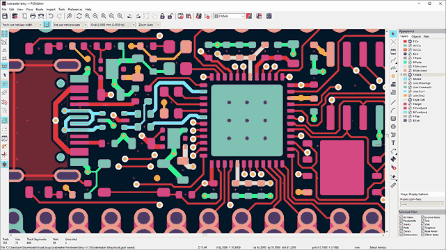
PCB Layout
Board Outline and Zones
Draw the board outline. Switch to the Edge.Cuts layer and draw a rectangle 55mm x 20mm. Round the corners with 1mm radius fillets if desired.
Create the GND zone on In1.Cu. Select Add Filled Zone, pick the In1.Cu (GND) layer, and assign it to the GND net. Draw the zone to cover the entire board area. Set the zone priority to 0.
Create the +3V3 zone on In2.Cu. Same process on In2.Cu, assigned to the +3V3 net.
Create GND pour on F.Cu and B.Cu. Add filled zones on both outer layers assigned to GND. These connect to the inner GND plane through vias and help with shielding. Set lower priority than any keep-out zones you add later.
Component Placement
Place the USB-C connector at one short edge of the board. Position the MCU in the center of the board with the exposed pad facing down (front side). Place the LDO and its capacitors between the USB connector and the MCU, keeping the power path short and direct.
Place decoupling capacitors on the back side of the board, directly beneath their corresponding VDD pins on the MCU. This is a major advantage of a 4-layer board: the capacitor pad on B.Cu connects through a via to the GND plane (In1.Cu), and through another via to the +3V3 plane (In2.Cu). The current loop from the power plane, through the via, through the capacitor, and back through the GND via is extremely short.
Place the HSE crystal within 5mm of the OSC_IN/OSC_OUT pins. Place the LSE crystal within 3mm of the OSC32 pins. Keep both crystal areas free of high-speed digital traces.
Place the SWD header at the opposite short edge from USB, or along one of the long edges. Place GPIO headers along both long edges of the board.
Placement priority order:
Priority
Component
Reason
1
USB-C connector
Fixed mechanical position at board edge
2
STM32F411
Central position, all signals radiate outward
3
HSE and LSE crystals
Must be close to MCU oscillator pins
4
Decoupling capacitors
Directly under/beside VDD pins
5
LDO and power caps
Short path from VBUS to MCU
6
SWD header
Edge position for probe access
7
GPIO headers
Board edges, last to place
Via Stitching
Via stitching means placing a regular pattern of vias connecting the GND zones on the outer layers to the inner GND plane. This serves multiple purposes: it reduces the impedance of the ground connection, it creates a Faraday cage effect that reduces EMI, and it provides thermal paths from the outer layers to the inner copper.
Add via stitching around the board perimeter. In KiCad, use Place > Via. Set the via net to GND. Place vias every 3 to 5mm around the board edge, inside the ground pour area. Stay at least 0.5mm from the board edge.
Add via stitching near USB traces. Place GND vias on both sides of the USB differential pair, spaced every 2 to 3mm. This shields the USB signals and provides a continuous ground reference.
Add via stitching near the MCU. Place GND vias around the MCU footprint, particularly near the exposed pad area. The exposed pad itself should have a grid of thermal vias (typically 4 to 9 vias in a 2x2 or 3x3 pattern) connecting to the inner GND plane for heat dissipation.
KiCad automatic via stitching. In KiCad 9, you can use Edit > Add Via Stitching to automate this. Set the via diameter to 0.3mm, drill to 0.15mm, and spacing to 3mm. Select the GND net and the target zones, then click OK.
USB Differential Pair Routing
This is the most critical routing on the board. USB 2.0 Full-Speed requires 90 ohm differential impedance.
Assign the USB net class. In Board Setup > Net Classes, verify that USB_DP and USB_DM are assigned to the “USB” net class with the correct trace width and spacing. For JLCPCB’s standard 4-layer stackup (0.21mm prepreg), approximately 0.2mm trace width and 0.15mm gap gives 90 ohm differential impedance. Use your fab house impedance calculator to confirm.
Route the differential pair. Select the Interactive Router and choose “Differential Pair” mode (or press D). Click on one pad of the USB D+/D- pair at the connector, and KiCad routes both traces simultaneously with matched spacing.
Keep traces on one layer. Route the entire USB pair on F.Cu. Avoid vias in the differential pair. Every via introduces an impedance discontinuity, and at USB Full-Speed (12 Mbps) this matters.
Length matching. The D+ and D- traces should be matched within 0.1mm. KiCad’s length tuning tool (accessible from the route menu) lets you add serpentine meanders to the shorter trace. For USB 2.0 Full-Speed, the tolerance is generous, but good practice is to match as closely as possible.
Keep the reference plane intact. Do not route other signals on the inner GND plane (In1.Cu) underneath the USB traces. The ground plane must be continuous under the differential pair for impedance control. If you must cross a signal, cross on In2.Cu (power plane) and add stitching vias nearby.
Termination. USB Full-Speed does not require external series termination resistors in most cases. The STM32’s internal drivers handle this. If you see signal integrity issues, you can add 22 ohm series resistors on D+ and D-.
Decoupling Capacitor Routing
The goal is to minimize the current loop area between each VDD pin, its decoupling capacitor, and GND. With 4-layer boards, the technique is straightforward: place the capacitor on the back side directly under the VDD pin, connect the capacitor’s power pad through a via to the +3V3 plane (In2.Cu), and connect its ground pad through a via to the GND plane (In1.Cu). The loop area becomes the distance between the two vias times the board thickness, which is extremely small.
Do not route long traces from decoupling caps to VDD pins. The via-to-plane connection should be the primary path. If the capacitor cannot sit directly below the VDD pin, keep the trace as short as possible and still use vias to both inner planes.
Design Rules for JLCPCB 4-Layer
Set these minimum design rules in Board Setup > Design Rules > Constraints:
Parameter
Minimum
Recommended
Trace width
0.09 mm
0.15 mm (0.2 mm for USB)
Trace spacing
0.09 mm
0.15 mm
Via drill
0.15 mm
0.2 mm
Via diameter
0.35 mm
0.45 mm
Annular ring
0.075 mm
0.1 mm
Copper to edge
0.2 mm
0.3 mm
These are slightly tighter than 2-layer rules because JLCPCB uses a different process for 4-layer boards. Always check the latest capabilities page before finalizing your design.
Running DRC
Fill all zones (Edit > Fill All Zones, or press B).
Open Inspect > Design Rules Checker.
Fix any clearance violations, unconnected nets, or minimum width violations.
Pay special attention to the inner planes. Look for unintended splits in the GND plane caused by traces routed on In1.Cu. The GND plane should be solid; remove any traces accidentally placed on it.
Manufacturing
The Gerber and drill file export process is the same as Lesson 3. This section covers 4-layer specifics.
4-Layer Options at JLCPCB
When ordering, select “4” for the layer count. JLCPCB offers a standard 4-layer stackup (JLC04161H-7628) at a reasonable price premium. For a board this size (55x20mm), expect to pay roughly 2x to 3x the cost of an equivalent 2-layer order (approximately 15 for 5 boards versus 5 for 2-layer). The cost difference decreases as board size increases because the per-board price for 4-layer has a higher fixed component but similar per-area scaling.
Impedance Control
If you need guaranteed impedance (rather than relying on typical stackup values), select “Yes” for impedance control in the JLCPCB order form. This adds cost (roughly 40 extra) but the fab house will adjust their process to hit your target impedance within a tighter tolerance (typically plus or minus 10%). For USB 2.0 Full-Speed, the standard stackup is usually close enough, so impedance control is optional.
Gerber Export Checklist
Make sure your Gerber export includes all six copper-related files:
File
KiCad Layer
F.Cu.gtl
F.Cu (Layer 1, top signals)
In1.Cu.g2
In1.Cu (Layer 2, GND plane)
In2.Cu.g3
In2.Cu (Layer 3, power plane)
B.Cu.gbl
B.Cu (Layer 4, bottom signals)
F.Mask, B.Mask
Solder masks
F.SilkS, B.SilkS
Silkscreen
Edge.Cuts
Board outline
Zip all Gerbers and drill files together. Upload to JLCPCB and verify the layer order in the Gerber viewer before placing the order.
Firmware: USB CDC Virtual COM Port
Once the board is assembled, verify it works by sending serial data over USB. The STM32F411 supports USB 2.0 Full-Speed natively on PA11/PA12.
STM32CubeMX Configuration
Open STM32CubeMX and create a new project for the STM32F411CEU6.
Under System Core > RCC, set High Speed Clock (HSE) to “Crystal/Ceramic Resonator” and Low Speed Clock (LSE) to “Crystal/Ceramic Resonator”.
Under Connectivity > USB_OTG_FS, set Mode to “Device_Only”.
Under Middleware > USB_DEVICE, set Class to “Communication Device Class (Virtual Port Com)”.
In the Clock Configuration tab, set the system clock to 96 MHz using the PLL with HSE as the source. The USB peripheral requires exactly 48 MHz, which the PLL can derive from a 25 MHz HSE crystal.
Generate the project code for your preferred toolchain (STM32CubeIDE, Makefile, or CMake).
Sending Data Over USB
In the generated project, open usbd_cdc_if.c. The function CDC_Transmit_FS() sends data to the host. Add a simple test in main.c:
/* main.c (inside the while(1) loop in main()) */
#include"usbd_cdc_if.h"
/* In main(), after MX_USB_DEVICE_Init() */
uint8_t msg[]="STM32F411 Black Pill alive\r\n";
uint32_t tick =0;
while (1)
{
if (HAL_GetTick()- tick >=1000)
{
tick =HAL_GetTick();
CDC_Transmit_FS(msg, sizeof(msg) -1);
}
}
Flash the firmware via SWD using an ST-Link or J-Link. Connect the board to a computer over USB-C. A virtual COM port should appear. Open a serial terminal at any baud rate (CDC ignores baud rate settings) and you should see:
STM32F411 Black Pill alive
STM32F411 Black Pill alive
STM32F411 Black Pill alive
On Linux, the device appears as /dev/ttyACM0. On Windows, it appears as a COM port in Device Manager. On macOS, look for /dev/tty.usbmodemXXXX.
Troubleshooting USB Enumeration
If the device does not appear on the host:
Check CC resistors. Without the 5.1 kOhm pull-downs on CC1 and CC2, the host will not supply VBUS power. Measure the voltage on VBUS; it should be 5V when the cable is connected.
Check the D+ pull-up. The host detects a Full-Speed device by seeing D+ pulled high. If using the internal pull-up, make sure the USB peripheral is initialized before the cable is connected (or add a short delay before USB init).
Verify the 48 MHz clock. USB requires exactly 48 MHz on the USB peripheral clock. If the PLL is misconfigured, the USB peripheral will not function. Double-check the CubeMX clock tree.
Check VCAP capacitor. A missing or wrong-value capacitor on the VCAP pin can cause the internal regulator to be unstable, leading to erratic behavior including USB failures.
Try a different cable. Some USB-C cables are charge-only and do not connect the data lines.
What You Have Learned
Lesson 4 Complete
KiCad skills:
Set up a 4-layer PCB stackup with inner ground and power planes
Routed USB 2.0 differential pairs with impedance-aware trace width and spacing
Used KiCad’s differential pair router for matched-length routing
Applied via stitching for ground plane integrity and EMI reduction
Placed decoupling capacitors on back side with via connections to inner planes
Electronics skills:
USB-C connector wiring for device mode (CC pull-downs, VBUS, data lines)
4-layer stackup design and its benefits for signal integrity
Impedance-controlled routing concepts (90 ohm differential for USB)
LDO power regulation with proper input/output capacitor selection
STM32F411 power supply design (VDD decoupling, VCAP, VDDA filtering)
Manufacturing skills:
4-layer Gerber export with inner layer files
JLCPCB 4-layer ordering options and cost considerations
Comments