Previous lessons accessed peripherals through polling loops or simple interrupts. That approach works for a single sensor, but it falls apart when you need continuous ADC sampling while pushing frames to a display and exchanging messages across a vehicle bus. This lesson introduces DMA for hands-free data movement, proper interrupt architecture for real-time responsiveness, and CAN bus for reliable multi-node communication. The project connects two STM32 Blue Pills over a CAN bus: one reads a potentiometer via DMA and transmits the value, the other receives it and drives an LED. #STM32 #CAN #DMA
What We Are Building
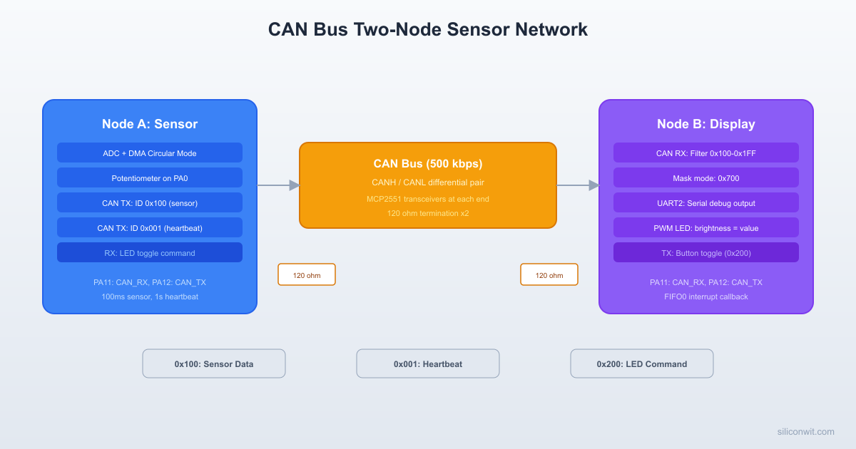
CAN Bus Sensor Network (Two Nodes)
Node A continuously samples a potentiometer through DMA-driven ADC and transmits the 12-bit value over CAN bus every 100 ms. It also sends a heartbeat frame every second. Node B receives the sensor data using hardware message filtering, prints it over UART, drives an LED with PWM proportional to the received value, and can send a command frame back to toggle Node A’s onboard LED. Both nodes handle CAN errors and recover from bus-off state automatically.
CAN Bus Two-Node Topology
┌────────────┐ ┌────────────┐
│ Node A │ CAN Bus │ Node B │
│ (Sensor) │ (twisted pair) │ (Display) │
│ │ │ │
│ STM32 ───┤ ┌──────────┐ ├─── STM32 │
│ PA11 RX ├──┤ MCP2551 │ │ PA11 RX │
│ PA12 TX ├──┤ CANH ────┼───┤ MCP2551 │
│ │ │ CANL ────┼───┤ CANH/CANL │
│ Pot(PA0) │ └──────────┘ │ LED(PA8) │
│ LED(PC13)│ [120R] [120R]│ BTN(PB0) │
└────────────┘ └────────────┘
Sensor data 0x100 ──> <── Command 0x200
Heartbeat 0x001 ──>
Project specifications:
Parameter
Value
Boards
2x Blue Pill (STM32F103C8T6)
CAN baud rate
500 kbps
CAN TX pin
PA12 (CAN_TX)
CAN RX pin
PA11 (CAN_RX)
Transceiver
MCP2551 (one per node)
Bus termination
120 ohm resistor at each end
Node A ADC
PA0 (ADC1 Channel 0, potentiometer)
Node A onboard LED
PC13 (active low)
Node B UART
PA2/PA3 (USART2 TX/RX)
Node B PWM LED
PA8 (TIM1 CH1)
Node B button
PB0 (send toggle command)
Message ID Scheme
Message ID
Direction
Content
0x001
Node A to bus
Heartbeat (1 byte uptime counter)
0x100
Node A to bus
Sensor data (2 bytes, 12-bit ADC value)
0x200
Node B to Node A
Command (1 byte: 0x01 = toggle LED)
0x300
Node A to bus
Status (1 byte: alarm flags)
Parts Needed
Part
Quantity
Notes
Blue Pill (STM32F103C8T6)
2
One per CAN node
MCP2551 CAN transceiver module
2
5V powered, one per node
120 ohm resistor
2
Bus termination at each end
10K potentiometer
1
Analog input for Node A
LED (any color)
1
PWM output on Node B
330 ohm resistor
1
Current limiting for LED
Push button
1
Command trigger on Node B
Breadboards
2
One per node
Jumper wires
20+
Assorted
DMA Controller Architecture
The STM32F103 has one DMA controller (DMA1) with 7 channels. Each channel is hardwired to specific peripheral requests. DMA moves data between memory and peripherals (or memory to memory) without CPU intervention. The CPU sets up source, destination, and transfer count, then the DMA controller handles every byte.
DMA Data Flow (ADC to Memory)
┌─────────────┐ DMA1 Ch1 ┌──────────┐
│ ADC1 │ (hardware │ SRAM │
│ Data Reg ├─────────────>│ Buffer │
│ (0x4001 │ request) │ adc_buf │
│ 244C) │ │ [N] │
└─────────────┘ └──────────┘
Source: fixed addr Dest: incrementing
Size: halfword (16-bit) Circular mode:
No CPU involvement restarts at [0]
DMA Transfer Modes
Mode
Source
Destination
Use Case
Peripheral to memory
Peripheral data register
SRAM buffer
ADC readings, UART RX, SPI RX
Memory to peripheral
SRAM buffer
Peripheral data register
UART TX, SPI TX, DAC output
Memory to memory
SRAM address
SRAM address
Buffer copy, frame buffer operations
Channel Assignments (DMA1)
Channel
Peripheral Request
Channel 1
ADC1
Channel 2
SPI1_RX, USART3_TX, TIM1_CH1
Channel 3
SPI1_TX, USART3_RX, TIM1_CH2
Channel 4
SPI2_RX, USART1_TX, TIM1_CH4
Channel 5
SPI2_TX, USART1_RX, TIM1_UP
Channel 6
USART2_RX, TIM1_CH3
Channel 7
USART2_TX
Circular Mode vs Normal Mode
In normal mode, DMA transfers the configured number of items and stops. You must reconfigure the channel to start another transfer. This suits one-shot operations like sending a fixed-length UART message.
In circular mode, DMA wraps back to the start of the buffer when it reaches the end and continues transferring indefinitely. This is ideal for continuous ADC sampling: the DMA keeps filling a buffer in a loop while the CPU reads completed values at its own pace.
Double Buffering with Half-Transfer Interrupts
DMA generates two interrupts during circular operation:
Half-transfer complete (HT): the first half of the buffer is filled
Transfer complete (TC): the second half is filled (and DMA wraps to start)
The CPU processes the first half while DMA fills the second half, and vice versa. This gives you uninterrupted streaming with no data loss.
Interrupt Architecture on Cortex-M3
The Nested Vectored Interrupt Controller (NVIC) on the STM32F103 uses 4 bits of priority, split between preemption priority and sub-priority based on the priority grouping setting.
Priority Rules
Group Setting
Preemption Bits
Sub-priority Bits
Preemption Levels
Group 4 (default)
4
0
16 levels, no sub-priority
Group 3
3
1
8 levels, 2 sub-priorities
Group 2
2
2
4 levels, 4 sub-priorities
A lower numeric value means higher urgency. An interrupt with preemption priority 1 can preempt a handler running at priority 2. Sub-priority only breaks ties when two interrupts pend simultaneously.
Common ISR Pitfalls
Interrupt Safety Checklist
Never call printf or HAL_Delay inside an ISR. Both rely on SysTick and can deadlock.
Keep ISRs short. Set a flag, copy data to a buffer, then return. Do processing in the main loop.
Mark shared variables volatile. The compiler can optimize away reads to variables modified in an ISR if they are not declared volatile.
Disable interrupts around multi-byte shared data. Reading a 32-bit value that an ISR modifies requires a critical section or atomic access.
CAN (Controller Area Network) is a multi-master, differential serial bus designed for noisy environments. It uses two wires (CANH and CANL) with differential signaling, making it resistant to electromagnetic interference. The bus requires 120 ohm termination resistors at each physical end.
Bus Electrical Levels
State
CANH
CANL
Differential
Recessive (logic 1)
2.5 V
2.5 V
0 V
Dominant (logic 0)
3.5 V
1.5 V
2 V
Dominant always wins over recessive. This property enables non-destructive bus arbitration: multiple nodes can start transmitting simultaneously, and the one with the lowest (highest-priority) message ID wins without any data corruption.
Standard CAN Frame Format
Field
Bits
Description
SOF
1
Start of frame (dominant)
Identifier
11
Message ID (lower value = higher priority)
RTR
1
Remote transmission request
IDE
1
Identifier extension (0 for standard)
DLC
4
Data length code (0 to 8 bytes)
Data
0 to 64
Payload (up to 8 bytes in classic CAN)
CRC
15
Cyclic redundancy check
ACK
2
Acknowledge slot + delimiter
EOF
7
End of frame (recessive)
Baud Rate Calculation
CAN bit timing divides each bit into time quanta (tq). For the STM32F103, CAN runs on APB1 (36 MHz max). To achieve 500 kbps:
Bit time = 1 / 500000 = 2 us
Time quanta per bit = SYNC_SEG(1) + BS1 + BS2
With prescaler = 4: tq = 4 / 36 MHz = 111.1 ns
Total tq per bit = 2 us / 111.1 ns = 18 tq
BS1 = 13 tq, BS2 = 4 tq, SYNC = 1 tq (total = 18)
Sample point at (1 + 13) / 18 = 77.8% (within recommended 75% to 80%)
SJW = 1 tq (resynchronization jump width)
Wiring: Two-Node CAN Network
Node A Wiring (Sensor Node)
Blue Pill Pin
Connects To
Function
PA0
Potentiometer wiper
ADC1 Channel 0 input
PA12
MCP2551 TXD
CAN TX
PA11
MCP2551 RXD
CAN RX
PC13
Onboard LED
Toggled by remote command
3.3V
Pot VCC, pull-ups
Power
GND
Pot GND, MCP2551 GND
Ground
5V
MCP2551 VCC
Transceiver power (5V required)
Node B Wiring (Display Node)
Blue Pill Pin
Connects To
Function
PA12
MCP2551 TXD
CAN TX
PA11
MCP2551 RXD
CAN RX
PA8
LED (through 330 ohm)
PWM output (TIM1 CH1)
PA2
USB-Serial RX
USART2 TX (debug output)
PA3
USB-Serial TX
USART2 RX
PB0
Push button to GND
Command trigger (pull-up enabled)
5V
MCP2551 VCC
Transceiver power
GND
MCP2551 GND, LED GND, button GND
Ground
MCP2551 Transceiver Wiring (Same for Both Nodes)
MCP2551 Pin
Connects To
TXD
STM32 PA12 (CAN_TX)
RXD
STM32 PA11 (CAN_RX)
VCC
5V
GND
GND
CANH
CAN bus CANH wire
CANL
CAN bus CANL wire
Rs
GND (high-speed mode) or 10K to GND (slope control)
Place a 120 ohm resistor between CANH and CANL at each node (both ends of the bus).
Create new project for STM32F103C8T6 in STM32CubeIDE.
Enable CAN: Under Connectivity, enable CAN. Set Prescaler = 4, Time Quanta in Bit Segment 1 = 13, Time Quanta in Bit Segment 2 = 4, ReSynchronization Jump Width = 1. This gives 500 kbps at 36 MHz APB1.
Enable ADC1: Under Analog, enable ADC1 Channel 0 (PA0). Set Continuous Conversion Mode = Enabled, DMA Continuous Requests = Enabled.
Enable DMA for ADC1: In the DMA Settings tab of ADC1, add DMA1 Channel 1. Set Mode = Circular, Data Width = Half Word (16-bit).
Configure TIM3: Under Timers, enable TIM3 with a 100 ms period. Prescaler = 7199 (timer clock 72 MHz / 7200 = 10 kHz), Counter Period = 999 (10000 / 1000 = 10 Hz, i.e. 100 ms). Note: TIM3 is on APB1, and since APB1 prescaler is /2, the timer clock is multiplied by 2, giving 72 MHz (not 36 MHz). Enable the update interrupt.
Configure PC13: Set as GPIO Output (onboard LED).
Set NVIC priorities: CAN RX0 interrupt = priority 1, DMA1 Channel 1 = priority 2, TIM3 = priority 3.
Generate code and open main.c.
Node B Configuration
Create new project for STM32F103C8T6.
Enable CAN: Same baud rate settings as Node A (Prescaler = 4, BS1 = 13, BS2 = 4, SJW = 1).
Enable USART2: Under Connectivity, enable USART2 in Asynchronous mode. Baud rate = 115200. TX = PA2, RX = PA3.
Enable TIM1 CH1 PWM: Under Timers, enable TIM1 Channel 1 as PWM Generation. Prescaler = 71 (72 MHz / 72 = 1 MHz), Counter Period = 999 (1 kHz PWM).
Configure PB0: Set as GPIO Input with internal pull-up.
Set NVIC priorities: CAN RX0 interrupt = priority 1, USART2 = priority 3.
Generate code.
Node A: Sensor Node Code
CAN Initialization and Filter Setup
can_config.c (Node A)
/* CAN filter configuration - accept all messages for Node A */
voidCAN_FilterConfig(void)
{
CAN_FilterTypeDef filter;
filter.FilterBank=0;
filter.FilterMode= CAN_FILTERMODE_IDMASK;
filter.FilterScale= CAN_FILTERSCALE_32BIT;
filter.FilterIdHigh=0x0000;
filter.FilterIdLow=0x0000;
filter.FilterMaskIdHigh=0x0000;
filter.FilterMaskIdLow=0x0000;
filter.FilterFIFOAssignment= CAN_RX_FIFO0;
filter.FilterActivation= ENABLE;
filter.SlaveStartFilterBank=14;
HAL_CAN_ConfigFilter(&hcan, &filter);
}
DMA ADC Setup
adc_dma.c (Node A)
/* Global variables */
volatileuint16_tadc_dma_buffer[4]; /* DMA fills this continuously */
/* Send sensor data every 100 ms (timer period) */
CAN_SendSensorData((uint16_t)adc_averaged);
/* Send heartbeat every 1 second (every 10th timer tick) */
heartbeat_tick++;
if (heartbeat_tick >=10) {
heartbeat_tick =0;
heartbeat_counter++;
CAN_SendHeartbeat(heartbeat_counter);
}
}
}
Node A main() Function
main.c (Node A)
intmain(void)
{
HAL_Init();
SystemClock_Config();
MX_GPIO_Init();
MX_DMA_Init();
MX_ADC1_Init();
MX_CAN_Init();
MX_TIM3_Init();
/* Configure CAN filter */
CAN_FilterConfig();
/* Start CAN peripheral */
HAL_CAN_Start(&hcan);
HAL_CAN_ActivateNotification(&hcan,
CAN_IT_RX_FIFO0_MSG_PENDING |
CAN_IT_ERROR_WARNING |
CAN_IT_ERROR_PASSIVE |
CAN_IT_BUSOFF |
CAN_IT_LAST_ERROR_CODE);
/* Start DMA-based ADC (circular mode) */
ADC_DMA_Start();
/* Start 100 ms timer */
HAL_TIM_Base_Start_IT(&htim3);
while (1) {
/* Toggle onboard LED if commanded by Node B */
if (led_toggle_request) {
HAL_GPIO_TogglePin(GPIOC, GPIO_PIN_13);
led_toggle_request =0;
}
/* Check for bus-off and attempt recovery */
uint32_t error =HAL_CAN_GetError(&hcan);
if (error & HAL_CAN_ERROR_BOF) {
HAL_CAN_Stop(&hcan);
HAL_Delay(100);
HAL_CAN_Start(&hcan);
HAL_CAN_ActivateNotification(&hcan,
CAN_IT_RX_FIFO0_MSG_PENDING |
CAN_IT_ERROR_WARNING |
CAN_IT_ERROR_PASSIVE |
CAN_IT_BUSOFF |
CAN_IT_LAST_ERROR_CODE);
}
HAL_Delay(10);
}
}
Node B: Display Node Code
CAN Filter Configuration (Mask Mode)
Node B uses mask mode filtering to accept only messages with IDs in the range 0x100 to 0x1FF (sensor data) and the heartbeat ID 0x001. Two filter banks handle this.
if (button_prev == GPIO_PIN_SET && button_now == GPIO_PIN_RESET) {
CAN_SendToggleCommand();
printf("Sent toggle command\r\n");
}
button_prev = button_now;
/* Bus-off recovery */
uint32_t error =HAL_CAN_GetError(&hcan);
if (error & HAL_CAN_ERROR_BOF) {
printf("CAN bus-off, recovering...\r\n");
HAL_CAN_Stop(&hcan);
HAL_Delay(100);
HAL_CAN_Start(&hcan);
HAL_CAN_ActivateNotification(&hcan,
CAN_IT_RX_FIFO0_MSG_PENDING |
CAN_IT_ERROR_WARNING |
CAN_IT_BUSOFF);
}
HAL_Delay(10);
}
}
CAN Error Handling
The bxCAN peripheral tracks three error counters and transitions through error states automatically:
State
TEC / REC
Behavior
Error Active
Both below 128
Normal operation, sends active error flags
Error Passive
Either at 128 or above
Sends passive error flags, waits longer between retransmits
Bus Off
TEC at 256 or above
Node disconnects from bus, requires 128 x 11 recessive bits to rejoin
TEC is the Transmit Error Counter and REC is the Receive Error Counter. You can read both from the CAN ESR register:
error_check.c
voidCAN_PrintErrorCounters(void)
{
uint32_t esr =hcan.Instance->ESR;
uint8_t tec = (esr >>16) &0xFF;
uint8_t rec = (esr >>24) &0xFF;
printf("TEC: %u REC: %u\r\n", tec, rec);
}
CubeMX Project Structure
DirectoryNodeA_CAN/
DirectoryCore/
DirectoryInc/
main.h
stm32f1xx_hal_conf.h
stm32f1xx_it.h
ring_buffer.h
DirectorySrc/
main.c
stm32f1xx_hal_msp.c
stm32f1xx_it.c
system_stm32f1xx.c
DirectoryDrivers/
DirectoryCMSIS/
…
DirectorySTM32F1xx_HAL_Driver/
…
NodeA_CAN.ioc
DirectoryNodeB_CAN/
DirectoryCore/
DirectoryInc/
main.h
stm32f1xx_hal_conf.h
stm32f1xx_it.h
DirectorySrc/
main.c
stm32f1xx_hal_msp.c
stm32f1xx_it.c
system_stm32f1xx.c
DirectoryDrivers/
DirectoryCMSIS/
…
DirectorySTM32F1xx_HAL_Driver/
…
NodeB_CAN.ioc
Testing the Network
Flash Node A with its firmware using ST-Link.
Flash Node B with its firmware using the same ST-Link (move the SWD cable between boards).
Connect a serial terminal (115200 baud) to Node B’s USART2 (PA2). You should see ADC values and heartbeat messages printed every 100 ms and 1 second respectively.
Turn the potentiometer on Node A. The ADC value printed on Node B should change smoothly from 0 to 4095, and the LED on Node B should vary in brightness.
Press the button on Node B. Node A’s onboard LED (PC13) should toggle.
Disconnect one termination resistor to observe CAN errors. The error counters will rise, and you may see bus-off recovery messages.
Production Notes
Moving to Production
CAN bus wiring: Use twisted pair cable for CANH and CANL. Keep stub lengths under 30 cm at each node tap. For runs longer than a few meters, use shielded cable with the shield grounded at one end.
Termination: Always 120 ohm at each physical end of the bus. In a two-node setup, both nodes are endpoints. In a multi-node linear bus, only the two endpoints get terminators.
EMC considerations: Add common-mode chokes on CANH/CANL at each node for production designs. Place decoupling capacitors (100 nF) close to the MCP2551 VCC pin. Consider ESD protection diodes (e.g., PESD1CAN) on CANH/CANL for automotive environments.
CAN FD upgrade path: The STM32F103 bxCAN peripheral supports classic CAN only (up to 1 Mbps, 8 bytes payload). For CAN FD (up to 8 Mbps, 64 bytes payload), consider the STM32G4 or STM32H7 families which include the FDCAN peripheral. The HAL API is similar, so the application logic ports with minimal changes.
DMA priority: In production firmware, assign DMA priorities carefully. ADC DMA should be high priority to avoid overrun. SPI DMA for displays can be medium priority since dropping a display frame is less critical than losing sensor data.
What You Learned
Lesson 9 Summary
DMA skills:
DMA controller channel assignments on the STM32F1
Circular mode for continuous ADC sampling without CPU intervention
Half-transfer and transfer-complete interrupts for double buffering
Interrupt architecture:
NVIC priority grouping (preemption vs sub-priority)
ISR safety rules: no printf, keep handlers short, use volatile for shared data
Ring buffer pattern for interrupt-safe data transfer
CAN bus skills:
Differential signaling, bus arbitration, frame format, bit timing calculation
bxCAN peripheral configuration: prescaler, BS1, BS2 for 500 kbps
Transmit mailboxes and receive FIFOs
Mask mode and list mode filter configuration
Error state machine: active, passive, bus-off, and recovery
System integration:
DMA ADC feeding data into CAN transmit on a timer interrupt
Two-node communication with bidirectional messaging
MCP2551 transceiver wiring with proper termination
Comments