You have now seen every major building block: logic gates perform Boolean operations, flip-flops store bits, counters keep time, memory holds data and code, buses move information, and ADCs bridge the analog world. This final lesson shows how all of these components are organized inside a microcontroller. When you write int x = 5; in C, a specific sequence of events unfolds in hardware: the instruction is fetched from Flash, decoded into control signals, executed in the ALU, and the result is stored in SRAM. Understanding this chain makes you a more effective embedded programmer. #CPUArchitecture #MicrocontrollerDesign #EmbeddedHardware
Von Neumann vs Harvard Architecture
Von Neumann Architecture
In the Von Neumann model, program instructions and data share the same memory and the same bus:
┌─────────┐ ┌───────────────────┐
│ │ │ Memory │
│ CPU │══════│ (code + data) │
│ │ │ │
└─────────┘ └───────────────────┘
single bus
Properties:
One bus for both instructions and data
Simpler design, fewer wires
Cannot fetch an instruction and access data simultaneously (the “Von Neumann bottleneck”)
Used in most desktop and server processors
Harvard Architecture
In the Harvard model, instructions and data have separate memories and separate buses:
┌─────────┐ ┌───────────────────┐
│ │══════│ Program Memory │
│ CPU │ │ (Flash) │
│ │══════│ Data Memory │
│ │ │ (SRAM) │
└─────────┘ └───────────────────┘
two separate buses
Properties:
Separate buses for instructions and data
Can fetch the next instruction while accessing data (parallelism)
Higher performance for a given clock speed
Used in most microcontrollers (AVR, PIC)
Modified Harvard (ARM Cortex-M)
ARM Cortex-M processors use a modified Harvard architecture: instructions and data have separate buses inside the CPU, but they share a unified memory map externally. The AHB bus matrix allows simultaneous instruction fetch and data access to different memory regions.
┌──────────────────┐
│ AHB Bus Matrix │
┌─────────┐ │ │ ┌───────┐
│ Cortex │═I-bus═│ │═════│ Flash │
│ -M │═D-bus═│ │═════│ SRAM │
│ CPU │═S-bus═│ │═════│Periph │
└─────────┘ └──────────────────┘ └───────┘
I-bus (Instruction): fetches instructions from Flash
D-bus (Data): reads/writes data from SRAM and peripherals
S-bus (System): debug access, DMA
This is why the STM32 can execute code from Flash at full speed while simultaneously reading data from SRAM. The bus matrix arbitrates when both buses try to access the same memory region.
Inside the CPU
Block Diagram
A simplified microcontroller CPU contains these core components:
The Program Counter holds the address of the next instruction to fetch. After each instruction is fetched, the PC automatically increments to point to the following instruction.
On ARM Cortex-M, the PC is register R15. It always contains the address of the current instruction plus 4 (due to the pipeline prefetch).
Branch instructions (B, BL, BX) modify the PC directly, causing execution to jump to a different address. This is how if, while, and function calls work at the hardware level.
Instruction Register and Decoder
The instruction fetched from Flash is placed in the Instruction Register. The Control Unit decodes it to determine:
What operation to perform (add, subtract, load, store, branch)
Which registers are the source and destination
Whether memory access is needed
What addressing mode to use
The decoder is a combinational logic circuit (built from gates, like the decoders in Lesson 3) that converts the instruction’s binary encoding into control signals for the ALU, register file, and bus interface.
Register File
The register file is a small, fast memory inside the CPU. ARM Cortex-M3 has 16 general-purpose 32-bit registers:
Register
Name
Purpose
R0-R3
Arguments/results
Function parameters and return values
R4-R11
General purpose
Callee-saved (preserved across function calls)
R12
IP
Intra-procedure scratch register
R13
SP
Stack Pointer
R14
LR
Link Register (return address for function calls)
R15
PC
Program Counter
Each register is a 32-bit parallel load register (Lesson 4). On each clock cycle, the register file can typically supply two source operands and accept one result.
Arithmetic Logic Unit (ALU)
The ALU performs arithmetic and logic operations. It takes two inputs (from the register file) and produces one output plus status flags.
Operations the ALU performs:
Category
Operations
Built From
Arithmetic
ADD, SUB, MUL
Adders (Lesson 3), subtractors
Logic
AND, OR, XOR, NOT
Logic gates (Lesson 2)
Shift
LSL, LSR, ASR, ROR
Shift registers (Lesson 4)
Compare
CMP (subtract without storing result)
Adder + flag logic
The ALU is the culmination of everything you learned in Lessons 2 and 3: it is a large combinational circuit that selects the appropriate operation using multiplexers and performs it using gate networks and adders.
Status Flags
The ALU sets four condition flags after each operation:
Flag
Name
Set When
N
Negative
Result is negative (MSB = 1)
Z
Zero
Result is zero
C
Carry
Unsigned overflow (carry out of MSB)
V
Overflow
Signed overflow (result does not fit in signed range)
Conditional branch instructions (BEQ, BNE, BCS, BCC) check these flags to decide whether to branch. This is how if (x == 0) works: the compiler generates a compare instruction (which sets flags) followed by a conditional branch.
The Instruction Execution Cycle
Fetch-Decode-Execute
Every instruction goes through three stages:
Fetch: The CPU puts the PC value on the address bus, reads the instruction from Flash memory, and stores it in the instruction register. The PC increments.
Decode: The control unit examines the instruction bits and generates control signals. It determines which ALU operation to perform, which registers to read, and where to store the result.
Execute: The ALU performs the operation. The result is written to the destination register (or to memory via the data bus).
Pipelining
To improve throughput, the CPU overlaps these stages. While one instruction executes, the next one is being decoded, and the one after that is being fetched:
Clock: 1 2 3 4 5 6
Instr 1: Fetch Decode Execute
Instr 2: Fetch Decode Execute
Instr 3: Fetch Decode Execute
Instr 4: Fetch Decode Execute
The ARM Cortex-M3 has a 3-stage pipeline. This means three instructions are “in flight” simultaneously. The pipeline is filled during the first three cycles, and after that, one instruction completes every clock cycle.
Pipeline hazards: When a branch instruction changes the PC, the instructions already in the pipeline (fetched from the wrong address) must be discarded. This is called a pipeline flush and wastes 2 clock cycles on Cortex-M3. This is why branch-heavy code (many if statements) can be slower than linear code.
What Happens When You Write int x = 5;
Let us trace this C statement through the entire chain, from source code to hardware.
Step 1: Compilation
The C compiler translates int x = 5; into ARM assembly. If x is a local variable:
MOV R0, #5; Load the immediate value 5 into register R0
STR R0, [SP, #4] ; Store R0 to the stack (SRAM) at offset 4 from SP
Step 2: Assembly to Machine Code
The assembler converts these mnemonics to binary machine code:
MOV R0, #5 → 0xF04F 0x0005 (Thumb-2 encoding)
STR R0, [SP, #4] → 0x9001 (Thumb encoding)
These binary values are stored in Flash memory.
Step 3: Fetch
The CPU places the PC value (say, 0x08000100) on the I-bus address lines. The Flash controller responds with the instruction word 0xF04F0005. The instruction register captures it.
Step 4: Decode
The control unit decodes 0xF04F0005 as “MOV R0, #5”:
Operation: move immediate value to register
Destination: R0
Immediate value: 5
Control signals are generated to:
Route the immediate value (5) to the ALU input
Set the ALU to pass-through mode
Enable write to R0 in the register file
Step 5: Execute
The ALU receives the value 5 and passes it through. The result (5) is written to R0 on the next clock edge. The register file (built from D flip-flops, Lesson 4) captures the value.
Step 6: Store to SRAM
The next instruction (STR R0, [SP, #4]) stores the value in R0 to SRAM:
The CPU calculates the address: SP + 4 (stack pointer plus offset)
The address goes on the D-bus address lines
The value in R0 (5) goes on the D-bus data lines
The write control signal is asserted
The SRAM at that address latches the value
The variable x now exists as the value 5 stored in a specific SRAM location, addressable by SP + 4.
The Stack
What Is the Stack?
The stack is a region of SRAM used for:
Local variables: function variables that exist only during the function’s execution
Return addresses: when a function is called, the return address (next instruction after the call) is saved on the stack
Saved registers: registers that a function must preserve are pushed to the stack on entry and popped on exit
How the Stack Works
The Stack Pointer (SP, R13) points to the top of the stack. On ARM Cortex-M, the stack grows downward (toward lower addresses):
High address ┌──────────────┐
│ │ (unused stack space)
│ │
├──────────────┤ ← SP (after push)
│ Saved R4 │
├──────────────┤
│ Saved LR │
├──────────────┤
│ Local var x │
├──────────────┤
│ Local var y │
├──────────────┤ ← SP (current)
│ │ (free stack space)
Low address └──────────────┘
PUSH decrements SP and stores a value. POP loads a value and increments SP.
Stack Overflow
If the stack grows too large (deep recursion, large local arrays), it can overwrite other data in SRAM. This is a stack overflow, and it causes unpredictable behavior, crashes, or silent data corruption. On MCUs with small SRAM (2 KB on ATmega328P), stack overflow is a real concern.
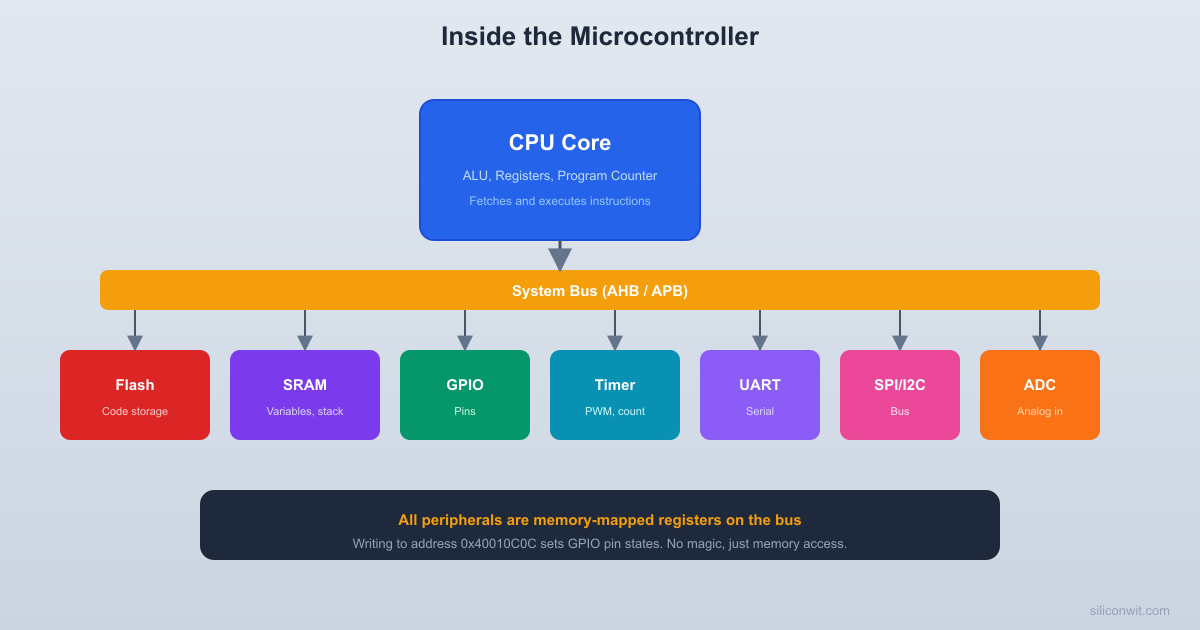
Memory-Mapped I/O
The Key Insight
On ARM Cortex-M (and most modern MCUs), peripheral registers are assigned specific addresses in the memory map, just like SRAM locations. The CPU accesses them using the same load/store instructions.
The CPU does not distinguish between these two operations. It puts the address on the bus, and the decoder logic (Lesson 3) routes the data to either SRAM or the GPIO peripheral.
How Writing to a Register Controls Hardware
When you write GPIOA->ODR = 0x0001;:
The compiler generates a STR instruction to address 0x4001080C.
The CPU places 0x4001080C on the address bus.
The AHB bus matrix routes the transaction to APB2 (where GPIO lives).
The address decoder enables GPIOA.
Within GPIOA, the offset 0x0C selects the ODR (Output Data Register).
The data 0x0001 is latched into the ODR register (a set of D flip-flops).
Bit 0 of the ODR drives the output buffer of pin PA0.
PA0 goes high (3.3V on the physical pin).
The entire chain, from C code to a pin changing state, involves: compiler, assembler, Flash storage, instruction fetch, decode, execute, bus transaction, address decoding, register latch, and output buffer. Every component you studied in this course plays a role.
Interrupts and the Vector Table
Why Interrupts?
Polling (checking a condition in a loop) wastes CPU time. Interrupts allow hardware events to pause the current code, handle the event, and return:
// Polling (wastes CPU time)
while (!(USART1->SR & (1<<5))) { } // Wait for RXNE flag
uint8_t data = USART1->DR;
// Interrupt (CPU does other work until data arrives)
voidUSART1_IRQHandler(void) {
uint8_t data =USART1->DR; // Called automatically when data arrives
}
How Interrupts Work in Hardware
Event occurs: A peripheral (timer overflow, UART receive, GPIO edge) sets an interrupt request flag.
NVIC arbitration: The Nested Vectored Interrupt Controller checks the interrupt’s priority against the current execution priority. If the new interrupt has higher priority, it proceeds.
Context save: The CPU pushes R0-R3, R12, LR, PC, and xPSR onto the stack (8 registers, automatically in hardware on Cortex-M). This takes 12 clock cycles.
Vector fetch: The CPU reads the interrupt vector table to find the address of the handler function. The vector table is an array of function pointers at the start of Flash memory.
Handler execution: The CPU jumps to the handler function and executes it.
Context restore: When the handler returns (BX LR with a special EXC_RETURN value), the CPU pops the saved registers from the stack and resumes the interrupted code.
The Vector Table
  Interrupt vector table (start of Flash)
  Address     Content  0x08000000  ┌───────────────────────┐              │ Initial SP value      │  0x08000004  ├───────────────────────┤              │ Reset handler addr    │ ← entry  0x08000008  ├───────────────────────┤              │ NMI handler addr      │  0x0800000C  ├───────────────────────┤              │ HardFault handler     │              ├───────────────────────┤              │ ...                   │  0x080000B4  ├───────────────────────┤              │ TIM2 handler addr     │              ├───────────────────────┤              │ ...                   │  0x080000D8  ├───────────────────────┤              │ USART1 handler addr   │              └───────────────────────┘
  Each entry is a 32-bit function pointer.
The vector table is stored at the beginning of Flash (address 0x08000000 on STM32):
Offset
Vector
Description
0x0000
Initial SP
Stack pointer value loaded at reset
0x0004
Reset
Address of the reset handler (entry point)
0x0008
NMI
Non-Maskable Interrupt handler
0x000C
HardFault
Hardware fault handler
…
…
…
0x00B4
TIM2
Timer 2 interrupt handler
0x00D8
USART1
USART1 interrupt handler
…
…
…
When the MCU powers on, it reads the initial SP from offset 0x0000 and the reset handler address from offset 0x0004. The program starts executing from the reset handler. This is why the linker script must place the vector table at the correct address.
Interrupt Latency
On ARM Cortex-M3, the worst-case interrupt latency (from event to first handler instruction) is 12 clock cycles. At 72 MHz, this is about 167 ns. This deterministic latency is what makes Cortex-M suitable for real-time applications.
Exercises
Exercise 1: Instruction Trace
The following ARM assembly code executes. Trace the register values after each instruction:
MOV R0, #10; R0 = ?
MOV R1, #3; R1 = ?
ADD R2, R0, R1 ; R2 = ?
SUB R3, R0, R1 ; R3 = ?
AND R4, R0, R1 ; R4 = ?
Solution
Instruction
R0
R1
R2
R3
R4
MOV R0, #10
10
-
-
-
-
MOV R1, #3
10
3
-
-
-
ADD R2, R0, R1
10
3
13
-
-
SUB R3, R0, R1
10
3
13
7
-
AND R4, R0, R1
10
3
13
7
2
For AND: 10 = 1010, 3 = 0011, AND = 0010 = 2.
Exercise 2: Memory-Mapped I/O
On an STM32F103, GPIOB base address is 0x40010C00. The ODR offset is 0x0C. Write a C expression that sets pin PB5 high without changing other pins.
The |= (OR) operation sets bit 5 without changing other bits. The address 0x40010C0C routes through the bus matrix to APB2, then to the GPIOB peripheral, then to the ODR register.
Exercise 3: Stack Depth
A function foo() has 3 local uint32_t variables and calls bar(), which has 2 local uint32_t variables. Ignoring saved registers and alignment padding, how many bytes of stack space do these two functions use together?
Solution
foo(): 3 variables x 4 bytes = 12 bytes, plus saved LR (4 bytes) = 16 bytes.
bar(): 2 variables x 4 bytes = 8 bytes, plus saved LR (4 bytes) = 12 bytes.
Total stack depth when bar() is executing (called from foo()): 16 + 12 = 28 bytes.
In practice, the compiler may also push callee-saved registers and add padding for alignment, so the actual usage is somewhat more.
Exercise 4: Interrupt Priority
Two interrupts fire simultaneously: TIM2 (priority 2) and USART1 (priority 1). On Cortex-M, lower priority numbers mean higher priority. Which handler executes first?
Solution
USART1 (priority 1) executes first because it has a lower priority number, meaning higher priority. TIM2 (priority 2) will be serviced after USART1’s handler returns, or will preempt if the NVIC is configured for it.
Putting It All Together
  Microcontroller block diagram (high level)
  ┌─────────────────────────────────────┐  │           MCU Chip                  │  │                                     │  │  ┌───────┐   ┌───────┐  ┌───────┐ │  │  │  CPU  │   │ Flash │  │ SRAM  │ │  │  │(Cortex│◄═►│(code) │  │(data) │ │  │  │  -M)  │   │ 64 KB │  │ 20 KB │ │  │  └───┬───┘   └───────┘  └───────┘ │  │      │   AHB / APB Bus             │  │  ════╪═══════════════════════════  │  │      │                             │  │  ┌───┴──┐ ┌─────┐ ┌────┐ ┌─────┐ │  │  │ GPIO │ │Timer│ │ADC │ │SPI/ │ │  │  │Ports │ │/PWM │ │    │ │I2C/ │ │  │  │      │ │     │ │    │ │UART │ │  │  └──┬───┘ └──┬──┘ └─┬──┘ └──┬──┘ │  └─────┼────────┼──────┼───────┼────┘     Pins     Pins   Analog   Serial                      Pins    Pins
This diagram shows how every lesson in the course maps to components inside a microcontroller:
Course Lesson
MCU Component
Lesson 1: Binary and Hex
Every register value, every address
Lesson 2: Logic Gates
ALU operations, decoder logic, multiplexers
Lesson 3: Combinational Logic
Address decoders, ALU arithmetic, GPIO mux
Lesson 4: Flip-Flops and Registers
CPU register file, SPI shift registers, peripheral registers
When you look at disassembly output or debug at the assembly level, you now understand what MOV, ADD, STR, LDR, and branch instructions do at the hardware level. This makes debugging HardFaults and optimization much more approachable.
Writing Efficient Code
Knowing that branch mispredictions flush the pipeline (2 wasted cycles on Cortex-M3) helps you understand why lookup tables can be faster than switch statements, and why small inline functions can outperform function calls.
Interrupt Design
Understanding the hardware context save (12 cycles), vector table lookup, and priority arbitration helps you write interrupt handlers that are fast and predictable. Keep handlers short. Do not call complex functions from ISRs.
Memory Layout
Knowing that Flash holds code and SRAM holds variables lets you interpret linker scripts, understand .text, .data, .bss, and .stack sections, and diagnose memory-related bugs (stack overflow, uninitialized data, Flash write issues).
Course Summary
You have now covered the complete digital foundation underlying every microcontroller:
Binary and hex are the language of hardware registers
Logic gates perform the Boolean operations your code compiles to
Combinational circuits route and decode signals
Flip-flops and registers store state
Counters keep time and generate waveforms
Memory stores your code and data
Buses move information between CPU, memory, and peripherals
ADCs and DACs bridge the analog and digital worlds
The CPU orchestrates everything through fetch, decode, execute
Every embedded programming course you take from here will build on this foundation. When you configure a timer, you know it is a counter with a prescaler. When you set up SPI, you know it is a pair of shift registers. When you write to a GPIO register, you know the data travels through address decoders and bus arbiters to reach a latch that drives a physical pin.
Comments