A sensor converts a physical quantity (temperature, light, pressure, strain) into an electrical signal. But that raw signal is rarely ready for a microcontroller’s ADC. It might be too small (millivolts), too noisy, have a DC offset, or change with the wrong polarity. Signal conditioning is the art of transforming the raw sensor output into a clean signal that fills the ADC’s input range and accurately represents the measured quantity. This lesson ties together everything you have learned in this course. #AnalogElectronics #Sensors #SignalConditioning
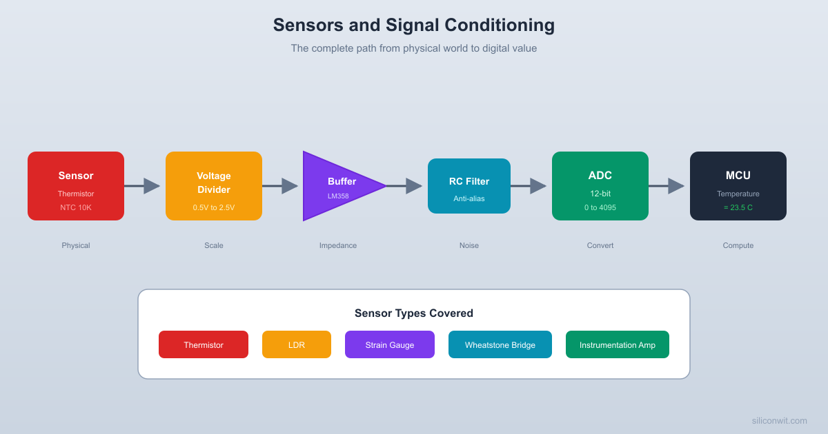
The Signal Conditioning Chain
Every sensor-to-digital conversion follows a similar path:
Sensor
Converts a physical quantity into an electrical signal (resistance change, voltage, current).
Excitation
Provides a stable voltage or current to the sensor (voltage divider, constant current source, Wheatstone bridge).
Amplification
Increases the signal amplitude to match the ADC input range (op-amp, instrumentation amplifier).
Filtering
Removes noise and prevents aliasing (RC low-pass filter, active filter).
Protection
Limits the voltage to the ADC’s safe input range (clamping diodes, Zener, series resistor).
ADC Sampling
Converts the conditioned analog signal to a digital value for processing by the MCU.
Each stage uses concepts from the previous lessons in this course. This lesson shows how they combine into a complete measurement system.
Common Sensor Types
Resistive Sensors
These sensors change their resistance in response to a physical quantity:
Sensor
Measures
Resistance Change
Typical Range
NTC thermistor
Temperature
Decreases with heat
100 ohm to 1M ohm
PTC thermistor
Temperature
Increases with heat
Varies
LDR (photoresistor)
Light intensity
Decreases with light
1k to 10M ohm
Strain gauge
Mechanical strain
Changes by 0.1 to 0.3%
120 or 350 ohm base
Potentiometer
Position/angle
Linear with position
Specified value
Flex sensor
Bending
Increases with bend
10k to 100k ohm
Resistive sensors are read by placing them in a voltage divider or Wheatstone bridge and measuring the resulting voltage.
Voltage-Output Sensors
Some sensors produce a voltage directly:
Sensor
Measures
Output Range
Thermocouple
Temperature
Microvolts to millivolts
Piezoelectric
Vibration, pressure
Millivolts (AC)
Hall effect
Magnetic field
0 to (ratiometric)
Microphone (electret)
Sound pressure
Millivolts (AC)
Photodiode
Light intensity
Nanoamps to microamps (current mode)
These typically require amplification and possibly level shifting before ADC input.
Thermistor Circuits
The NTC (Negative Temperature Coefficient) thermistor is the most common temperature sensor for hobbyist and embedded projects. Its resistance decreases as temperature increases, following an exponential relationship.
Thermistor in a Voltage Divider
The simplest thermistor circuit uses a fixed resistor and the thermistor in a voltage divider:
    VCC (3.3V)      |    [Rf] 10K (fixed)      |      +------> Vout (to ADC)      |    [NTC] 10K at 25C      |     GND
  Cold (0C):  NTC=27K, Vout=2.42V  Room (25C): NTC=10K, Vout=1.65V  Hot (50C):  NTC=3.6K, Vout=0.87V
When the thermistor is cold (high resistance), is close to . When hot (low resistance), drops toward 0V.
Choosing the Fixed Resistor
For maximum sensitivity, choose the fixed resistor equal to the thermistor’s resistance at the midpoint of your measurement range. For a 10k NTC thermistor at 25 degrees Celsius:
At 25C: ,
At 0C: ,
At 50C: ,
A 10k fixed resistor gives a useful voltage swing of about 0.47 over the 0 to 50C range.
Steinhart-Hart Equation
The relationship between thermistor resistance and temperature is non-linear. The Steinhart-Hart equation provides an accurate model:
Where:
is temperature in Kelvin
is thermistor resistance in ohms
, , are coefficients specific to the thermistor (from the datasheet)
A simpler (less accurate) approximation uses the B-parameter:
Where (25C), (resistance at ), and for a typical 10k NTC.
This calculation is typically done in software on the MCU after the ADC reads the voltage.
Light Dependent Resistor (LDR)
An LDR (photoresistor) changes resistance with light intensity. In darkness, resistance is very high (1M ohm or more). In bright light, resistance drops to a few hundred ohms.
LDR Voltage Divider
VCC ── R_fixed (10k) ──┬── V_out (to ADC)
│
LDR
│
GND
In bright light: LDR resistance is low, is low.
In darkness: LDR resistance is high, is high.
Swapping the LDR and fixed resistor inverts this relationship.
LDRs are slow (response time 10 to 100 ms) and not very accurate, but they are cheap and easy to use for light/dark detection, automatic brightness control, and simple light meters.
The Wheatstone Bridge
For sensors with very small resistance changes (like strain gauges, which change by only 0.1 to 0.3%), a simple voltage divider lacks sensitivity. The Wheatstone bridge solves this by measuring the difference between two voltage dividers.
Bridge Circuit
            VCC (5V)             |       ┌-----+-----┐       |            |     [R1] 350     [R2] 350       |            |  Va --+            +-- Vb       |            |     [R3] Sensor  [R4] 350     (strain gauge)  |       |            |       └-----+-----┘             |            GND
  Vbridge = Va - Vb  Balanced: Va = Vb, Vbridge = 0  Sensor change: small differential  output (millivolts)
The bridge output voltage is the difference between the two midpoints:
When the bridge is balanced (), the output is zero. A small change in one resistor (the sensor) produces a small but measurable differential voltage.
Strain Gauge Example
A strain gauge has a nominal resistance of 350 ohm and a gauge factor of 2. Under a strain of 1000 microstrain ():
That is a change of 0.2%. In a voltage divider with a 5V supply, this produces a voltage change of only about 5 mV, which is easily overwhelmed by noise. In a Wheatstone bridge with a differential amplifier, this signal can be cleanly extracted and amplified.
Bridge Sensitivity
For a single active element (quarter bridge, where one resistor is the sensor and the other three are fixed):
For the strain gauge example:
This small signal requires careful amplification.
Instrumentation Amplifier
The instrumentation amplifier (INA) is a specialized high-gain differential amplifier designed for measuring small signals in noisy environments. It amplifies the difference between its two inputs while rejecting common-mode noise.
Three Op-Amp Instrumentation Amplifier
The classic instrumentation amplifier uses three op-amps:
Two input buffer amplifiers (non-inverting configuration) provide high input impedance and initial gain
One difference amplifier subtracts the two buffered signals and provides the final output
The gain is typically set by a single resistor ():
Where is a fixed internal resistor value.
Dedicated INA ICs
For production designs, dedicated instrumentation amplifier ICs are preferred over discrete op-amp implementations:
Part
Gain Range
Supply
Key Feature
INA128
1 to 10,000
dual supply
General purpose, low noise
INA333
1 to 1,000
single supply
Low power, rail-to-rail
AD620
1 to 10,000
dual supply
Industry standard, low cost
INA219
Fixed
single supply
Integrated ADC, I2C output
For breadboard prototyping with the LM358, you can build a simple differential amplifier (Lesson 5) that works adequately for signals above 10 mV. For microvolt-level signals (thermocouples, strain gauges), a dedicated INA is necessary.
Signal Conditioning Design Process
Here is a systematic approach to designing a signal conditioning circuit:
Characterize the sensor output
What is the voltage range? What is the source impedance? Is the signal differential or single-ended? What is the frequency content?
Determine the ADC requirements
What is the ADC input range (0 to 3.3V, 0 to 5V)? What is the ADC resolution (10-bit, 12-bit)? What is the maximum source impedance the ADC can handle?
Calculate the required gain
Design the amplifier stage
Choose non-inverting for single-ended signals, differential/INA for bridge sensors. Select resistor values for the required gain.
Add filtering
Place a low-pass filter after the amplifier with cutoff frequency at or below . This serves as the anti-aliasing filter.
Add protection
Place series resistors (1k to 10k) and clamping diodes at the ADC input to protect against overvoltage. Many MCUs have internal clamping diodes, but external protection adds a safety margin.
Verify the design
Measure the output at known sensor values. Compare with your calculated expected values. Check noise level with an oscilloscope if available.
Practical Build: Complete Temperature Measurement Circuit
This project combines a thermistor voltage divider, an op-amp buffer, a non-inverting amplifier, and an RC filter into a complete signal conditioning chain.
Components Needed
Component
Quantity
Notes
Breadboard
1
From previous lessons
LM358 dual op-amp
1
DIP-8 package
NTC thermistor 10k ohm
1
Standard NTC
Resistors: 1k, 3.3k, 4.7k, 10k, 22k ohm
2 each
1% metal film preferred
Capacitor 100 nF ceramic
3
For decoupling and filtering
Capacitor 10 nF ceramic
1
For anti-aliasing filter
Potentiometer 10k ohm
1
For gain adjustment
5V regulated supply
1
LM1117 circuit from Lesson 6, or USB
Digital multimeter
1
DC voltage mode
Cup of hot water and ice water (optional)
1 each
For temperature range testing
Jumper wires
Several
Male-to-male
The Design
Goal: Read temperature from 0 to 100 degrees Celsius and output 0 to 3.3V for a 12-bit ADC.
Stage 1: Thermistor voltage divider
10k fixed resistor + 10k NTC thermistor
At 25C:
At 0C:
At 100C:
The voltage range is about 3.3V, which is convenient
Stage 2: Buffer (Op-amp A of LM358)
Voltage follower isolates the thermistor from the amplifier
Stage 3: Gain stage (Op-amp B of LM358)
Since the thermistor divider already produces approximately 0 to 3.3V over the 0 to 100C range, we can set the gain close to 1. For a narrower range (20 to 50C), we would increase the gain and add an offset.
For this build, use gain = 1 (second buffer) to demonstrate the full chain cleanly
Stage 4: Anti-aliasing filter
RC low-pass at the output: ,
This is adequate for temperature measurement (which changes slowly)
VCC Buffer Amplifier Filter
| ┌------┐ ┌------┐
[Rf] | | | | [R]3.3K
+------->|+ OUT-+---->|+ OUT-+--/\/\--+->ADC
| | | | | |
[NTC] +->|- ---┘ +->|- ---┘ [C]100nF
| | └------┘ | └------┘ |
GND | (LM358 A) | (LM358 B) GND
| |
(output to [R1]+[Rf pot]
inv. input) to GND
Build Steps
Build the regulated power supply
Use the 3.3V regulator from Lesson 6, or a 5V USB supply. Place 100 nF decoupling capacitors at the supply points.
Build the thermistor divider
Connect a 10k fixed resistor from VCC (use 3.3V if you want the output to stay within 3.3V range, or 5V and accept that some of the range will be above 3.3V) to a node. Connect the 10k NTC thermistor from that node to ground.
Connect the buffer
Wire the divider output to pin 3 (non-inverting input A) of the LM358. Connect pin 1 (output A) to pin 2 (inverting input A). Power the LM358 with VCC on pin 8, GND on pin 4, and a 100 nF decoupling capacitor.
Connect the amplifier/second buffer
Wire pin 1 (buffer output) to pin 5 (non-inverting input B). For a unity-gain buffer: connect pin 7 (output B) to pin 6 (inverting input B). For adjustable gain: connect a 10k resistor from pin 6 to GND, and a 10k potentiometer from pin 6 to pin 7.
Add the anti-aliasing filter
Connect a 3.3k resistor from pin 7 (amplifier output) to the final output node. Connect a 100 nF capacitor from the output node to ground.
Add protection (optional)
If connecting to a real MCU ADC, add a 1k series resistor at the very end, followed by two Schottky diodes: one from the signal to VCC (clamps high), one from GND to the signal (clamps low). This prevents the ADC input from exceeding the safe range.
Measure at room temperature
Record the voltage at the thermistor divider output, the buffer output, the amplifier output, and the filter output. They should all be very close (since gain is approximately 1). Typical room temperature reading with 3.3V supply: about 1.65V.
Test with hot water
Dip the thermistor in warm water (be careful with the wiring). The voltage should decrease (NTC thermistor: lower resistance when hot, lower voltage in the bottom position of the divider). Record the voltage.
Test with ice water
Dip the thermistor in ice water. The voltage should increase. Record the voltage.
Calculate temperature from voltage
Use the thermistor B-parameter equation to convert measured voltage back to temperature:
From the ADC voltage, calculate thermistor resistance:
From resistance, calculate temperature using the B-parameter equation
Verification Checklist
Measurement
Expected Value
Your Measurement
Divider output at room temp (~25C)
~1.65V (3.3V supply)
________
Buffer output
Same as divider
________
Amplifier output (gain=1)
Same as buffer
________
Filter output
Same as amplifier (DC)
________
Hot water (~50C) output
~0.56V (3.3V supply)
________
Ice water (~0C) output
~2.42V (3.3V supply)
________
Calculated resistance (room temp)
~10k ohm
________
Calculated temperature
~25C
________
Connecting to a Microcontroller
If you have an Arduino, STM32 Blue Pill, or any MCU with an ADC:
Connect the filter output to an ADC input pin
Connect the circuit ground to the MCU ground
Read the ADC value in your firmware
Convert ADC count to voltage:
Convert voltage to resistance:
Convert resistance to temperature using the Steinhart-Hart or B-parameter equation
Print the temperature to a serial terminal
This is exactly the signal path used in production temperature measurement systems, from industrial process control to weather stations to HVAC systems. The principles are identical whether you are building on a breadboard or designing a multi-layer PCB.
Noise Reduction Techniques
Hardware Techniques
Technique
How It Helps
Shielded cables
Blocks electromagnetic interference from reaching sensor wires
Twisted pair wiring
Cancels induced noise (both wires pick up the same noise, differential amplifier rejects it)
Proper grounding
Star ground topology prevents ground loops that inject noise
Decoupling capacitors
Provide clean local power to amplifier stages
Physical separation
Keep analog sensor circuits away from digital switching circuits, motors, and power supplies
Software Techniques
Technique
How It Helps
Averaging
Take N samples and compute the mean. Reduces random noise by
Median filtering
Take N samples and use the median. Rejects spike noise (outliers)
Exponential moving average
. Simple, memory-efficient low-pass filter
Oversampling
Sample at a higher rate than needed, then average. Each 4x oversampling adds 1 bit of effective resolution
The best approach combines both: hardware filtering removes noise before the ADC, and software filtering cleans up the remaining noise in the digital domain.
Common Mistakes
Watch Out For These
No buffer before the ADC: The ADC’s sampling capacitor draws current pulses that disturb high-impedance sources like voltage dividers. Buffer the signal with an op-amp voltage follower.
Missing anti-aliasing filter: Without a low-pass filter before the ADC, high-frequency noise aliases into the measurement band and cannot be removed by software.
Using a long wire to the sensor: Long wires act as antennas, picking up 50/60 Hz mains hum and RF interference. Keep wires short, use shielded cable for distances over 30 cm, and filter at the ADC input.
Ground loops: Connecting ground at multiple points in a circuit can create loops that inject noise. Use a single-point (star) ground connection.
Amplifier saturation: If the amplifier gain is too high, the output clips at the supply rail and you lose information. Always verify that the output stays within the supply range across the full sensor range.
Ignoring self-heating: Passing too much current through a thermistor heats it up, shifting the reading. Keep the excitation current low (below 1 mA for most NTC thermistors).
How This Connects to Embedded Systems
This Is What Happens Before the ADC Pin
Every analog sensor reading on every MCU in the world goes through some form of signal conditioning:
STM32 ADC projects: The ADC lessons in the STM32 course discuss source impedance, sampling time, and resolution. Now you understand the analog circuit that feeds the ADC and why those parameters matter.
IoT sensor nodes: Temperature, humidity, light, and air quality sensors all require signal conditioning. Some sensors (like the DHT22 or BME280) have built-in conditioning and output digital data. Others (thermistors, LDRs, strain gauges) require external conditioning.
Industrial measurement: Production systems use instrumentation amplifiers, precision voltage references, and Wheatstone bridges for accuracy. The principles are identical to what you built on your breadboard, just with tighter tolerances and more robust components.
PCB design for analog signals: On a PCB, analog signal traces must be short, routed away from digital signals, and surrounded by ground copper. The analog ground and digital ground are sometimes separated and connected at a single point near the ADC.
Calibration: Even with perfect signal conditioning, component tolerances introduce errors. Production systems include a calibration step where known reference values are measured and correction factors are stored in flash memory.
Course Summary
You have now covered the complete foundation of analog electronics for embedded systems:
Lesson
Core Concept
Embedded Connection
1. Voltage, Current, Resistance
Ohm’s law, KVL, KCL
GPIO current limits, pull-up resistors
2. Capacitors and RC Circuits
Time constants, energy storage
Decoupling, debouncing, RC timing
3. Diodes and Protection
Forward/reverse bias, flyback
Relay protection, reverse polarity, ESD
4. Transistors
BJT/MOSFET switching
Motor drivers, level shifting, power control
5. Op-Amps
Amplification, buffering
ADC source impedance, signal scaling
6. Power Supply Design
Regulation, decoupling
MCU power rails, battery efficiency
7. Filters
Frequency selection, anti-aliasing
ADC input filtering, noise rejection
8. Oscillators
RC and crystal timing
System clock, UART baud rate, watchdog
9. Sensors and Conditioning
Complete measurement chain
Everything before the ADC pin
These nine lessons give you the vocabulary and practical skills to understand, design, and debug the analog portions of any embedded system. When a circuit behaves unexpectedly, you now have the tools to measure, analyze, and fix the problem at the component level.
Comments