A microcontroller that runs on a noisy or unstable power supply will produce erratic ADC readings, random resets, corrupted flash writes, and unexplainable bugs. Power supply design is not glamorous, but it is the foundation that everything else depends on. This lesson covers the two main approaches to voltage regulation, teaches you to calculate thermal limits, and walks you through building a clean 3.3V supply from a 9V battery. #AnalogElectronics #PowerSupply #VoltageRegulation
Why Voltage Regulation Matters
Batteries discharge over time (a “9V” battery actually ranges from 9.6V fresh to about 6V near end of life). USB ports deliver 5V plus or minus 10%. Solar panels vary with sunlight. Wall adapters have ripple from the AC-to-DC conversion. None of these sources provide the stable, precise voltage that a microcontroller needs.
A voltage regulator takes a higher (and possibly noisy) input voltage and produces a stable, lower output voltage. The two main types are linear regulators and switching regulators.
Linear Regulators
A linear regulator works by acting as a variable resistor between the input and output. It continuously adjusts its internal resistance to maintain a constant output voltage, regardless of changes in input voltage or output current.
How They Work
Think of a linear regulator as an automatic faucet. You set the desired water pressure (output voltage), and the faucet adjusts its opening (internal resistance) to maintain that pressure regardless of how much the supply pressure changes.
The excess voltage is dissipated as heat:
This is the fundamental limitation of linear regulators: they waste power proportional to the voltage difference.
The 7805: Classic Linear Regulator
The 7805 is a fixed 5V linear regulator that has been in production since the 1970s. It requires at least 7V input (2V dropout) and can deliver up to 1A with adequate heatsinking.
Parameter
7805 Value
Output voltage
5.0V fixed
Dropout voltage
~2V
Maximum input
35V
Maximum output current
1A (with heatsink)
Quiescent current
~5 mA
Worked Example: 7805 Heat Dissipation
Running a 7805 from a 12V input at 500 mA:
That is significant heat. A TO-220 package without a heatsink can only dissipate about 1 to 2W before exceeding its maximum junction temperature. You would need a heatsink or a fan for this application.
Efficiency:
Nearly 60% of the input power is wasted as heat. This is acceptable for low-current applications but impractical for battery-powered systems.
LDO Regulators (Low Dropout)
An LDO (Low Dropout) regulator is a linear regulator with a very small minimum voltage difference between input and output. Where the 7805 needs 2V of headroom, an LDO might need only 0.2 to 0.5V.
                LM1117-3.3  Vin           ┌--------┐  (5-9V)        |        |  o---+---------|IN  OUT |---+---o Vout      |         |   GND  |   |     (3.3V)  C1 ===10uF    └---+----┘  === C2 10uF      |  |          |        |  |  C3 ===100nF       |       === C4 100nF      |             |        |      +-------------+--------+      |     GND
  C1,C3: input filtering  C2,C4: output stability (required!)
The LM1117-3.3
The LM1117-3.3 is a popular LDO that produces a fixed 3.3V output:
Parameter
LM1117-3.3 Value
Output voltage
3.3V fixed
Dropout voltage
~1.2V at 800 mA, ~0.6V at 100 mA
Maximum input
15V
Maximum output current
800 mA
Quiescent current
~5 mA
The dropout voltage decreases at lower currents, which is typical of LDOs.
When to Use an LDO
LDOs are ideal when:
The input-to-output voltage difference is small (e.g., 5V to 3.3V = 1.7V, well within LM1117 capability)
Output current is moderate (under 500 mA)
You need low output noise (linear regulators produce much less output noise than switching regulators)
Board space is limited (no inductor needed)
Cost must be minimal
LDOs are a poor choice when:
The input-to-output difference is large (e.g., 12V to 3.3V at high current wastes too much power)
Efficiency matters (battery life)
Output current exceeds 1A
LDO Thermal Calculation
Before using an LDO, always calculate the power dissipation and check the thermal limits.
Calculate power dissipation
Check the thermal resistance
Look up (junction-to-ambient thermal resistance) in the datasheet. For a TO-220 package without heatsink, this is about 50 C/W. For an SOT-223 surface mount, it is about 100 to 150 C/W.
Calculate junction temperature
Where is the ambient temperature. must stay below the maximum (usually 125 C).
Example: LM1117-3.3 in SOT-223 package, , , , :
This is below 125 C, so it works. But increasing current to 500 mA would push to , which exceeds the limit. You would need a larger package, a heatsink, or a switching regulator.
Switching Regulators
Switching regulators achieve much higher efficiency (typically 85 to 95%) by rapidly switching the input on and off and using an inductor and capacitor to smooth the output. They can step voltage down (buck), step it up (boost), or do both (buck-boost).
How They Work (Simplified)
A buck (step-down) switching regulator chops the input voltage into high-frequency pulses using a transistor switch, then smooths these pulses with an LC (inductor-capacitor) filter.
The switch opens and closes at a high frequency (typically 100 kHz to several MHz). The duty cycle (percentage of time the switch is on) determines the output voltage:
Input is 5V, output is 3.3V (small drop, moderate current)
Powering sensitive analog circuits (ADC reference, sensor amplifiers)
Board space is extremely limited
Total output current is under 500 mA
Low noise is critical
Input is 12V or 24V, output is 3.3V (large drop)
Battery-powered device where efficiency affects runtime
Output current exceeds 500 mA
You need to boost voltage (3.3V battery to 5V output)
Heat dissipation is a concern
Many designs use both: a switching regulator steps 12V down to 5V efficiently, then an LDO produces a clean 3.3V from the 5V rail for the microcontroller and analog circuits. This combines the efficiency of switching with the low noise of linear regulation.
              Buck              LDO  12V       Converter         LM1117  o---+--> [DCDC 5V] --+--> [3.3V] --> MCU      |    (efficient)  |   (low noise)      |                 |      |                 +--> 5V peripherals      |     GND
  Stage 1: 12V to 5V (switching, 90%)  Stage 2: 5V to 3.3V (linear, clean)
Decoupling and Bypassing
Decoupling capacitors are perhaps the most important aspect of power supply design for digital circuits. They provide a local energy reservoir near each IC, supplying instantaneous current during switching transients.
Why Decoupling Is Necessary
When a digital IC switches its output, it draws a sudden burst of current from the power supply. The trace (wire) between the power supply and the IC has inductance. This inductance resists sudden changes in current, causing a momentary voltage dip at the IC’s power pin:
A decoupling capacitor placed right at the IC’s power pin provides that burst current locally, bypassing the inductance of the power trace.
Decoupling Strategy
MCU IC
Vreg 100uF ┌-----------┐
out +---||---+ | |
| | | VCC1 VCC2
+----+----+ +---|---+ |
| | | 100nF 100nF
| 10uF | | | |
+--||--+ +-------|---+-GND+
| | | |
+------+----------+-------+
|
GND Bulk Per-pin
cap decoupling
For most MCU and digital circuits, use this three-tier approach:
Capacitor
Type
Placement
Purpose
100 nF (0.1 )
Ceramic (MLCC)
At each VCC/GND pin pair
High-frequency decoupling
1 to 10
Ceramic or tantalum
Near IC, one per IC
Mid-frequency decoupling
10 to 100
Electrolytic or ceramic
Near power input
Bulk energy storage
Placement matters more than value. A 100 nF capacitor 2 mm from the pin is far more effective than a 10 capacitor 20 mm away. On a PCB, route the decoupling capacitor directly between the VCC and GND pins with the shortest traces possible.
Breadboard Decoupling
On a breadboard, the long power rails have significant inductance. Reduce this by:
Placing capacitors as close as possible to each IC
Using short jumper wires
Running a separate ground wire directly from the IC to the power supply ground
Ripple and Noise
Ripple
Ripple is the residual AC voltage on top of the DC output. Every power supply has some ripple.
For a linear regulator, ripple comes from the input supply (typically from the rectifier filter capacitor) and is reduced by the regulator’s PSRR (Power Supply Rejection Ratio). The LM1117 has about 75 dB PSRR at 120 Hz, meaning input ripple is reduced by a factor of about 5600 at the output.
For a switching regulator, ripple comes from the switching action itself. Typical output ripple is 10 to 50 mV peak-to-peak, depending on the output capacitor and inductor values.
Noise
Noise is random voltage fluctuation, broader in spectrum than ripple. Linear regulators produce less noise than switching regulators. For precision ADC applications, the power supply noise must be less than 1 LSB (least significant bit) of the ADC:
For a 12-bit ADC with 3.3V reference:
Power supply noise must be well below 0.8 mV for full 12-bit accuracy. This is achievable with a good LDO and proper decoupling.
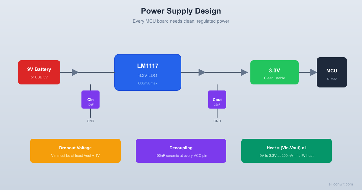
Practical Build: 3.3V Regulated Supply
Components Needed
Component
Quantity
Notes
Breadboard
1
From previous lessons
LM1117-3.3
1
TO-220 or SOT-223 package
7805 (optional)
1
TO-220, for comparison
9V battery + snap connector
1
Fresh battery preferred
Capacitor 10 electrolytic
2
25V or higher
Capacitor 100 nF ceramic
3
For decoupling
Capacitor 100 electrolytic
1
For bulk filtering
LED (red)
1
Power indicator
Resistor 1k ohm
1
For LED current limit
Resistors: 100, 220, 470 ohm
1 each
For load testing
Digital multimeter
1
DC voltage mode
Jumper wires
Several
Male-to-male
LM1117 Pinout (TO-220, facing label)
Pin
Function
1 (left)
GND/Adjust
2 (center)
Output (3.3V)
3 (right)
Input
Note: the LM1117 pinout is different from the 7805. The 7805 is Input, GND, Output (left to right). Always check the datasheet.
Build Steps
Place the LM1117-3.3
Insert the regulator into the breadboard with the tab facing away from you. Identify the three pins using the datasheet.
Connect the input capacitors
Place a 10 electrolytic capacitor from the input pin (pin 3) to ground. Place a 100 nF ceramic capacitor in parallel (same pins). The electrolytic handles low-frequency filtering and the ceramic handles high-frequency noise.
Connect the output capacitors
Place a 10 electrolytic capacitor from the output pin (pin 2) to ground. Place a 100 nF ceramic capacitor in parallel. The LM1117 datasheet specifically requires a minimum of 10 on the output for stability. Do not skip this.
Add the power indicator LED
Connect a 1k ohm resistor and red LED in series from the output to ground. This draws about 1.6 mA and confirms the regulator is producing voltage.
Connect the 9V battery
Connect the positive terminal to the input pin and the negative terminal to ground. The LED should light up immediately.
Measure the output voltage (no load)
Place your multimeter across the output. You should read 3.3V, plus or minus about 0.05V (within the regulator’s tolerance).
Load test with a resistor
Connect a 100 ohm resistor from the output to ground. This draws . Measure the output voltage again. It should remain at 3.3V (within tolerance).
Calculate power dissipation
With the 9V battery (actual voltage may be 8.5V) and 33 mA load:
The LM1117 should be barely warm.
Heavy load test
Replace the 100 ohm with a 22 ohm resistor ().
Measure the output voltage. It should still be close to 3.3V. The LM1117 will be warm to the touch. After about 30 seconds, measure the output again to confirm it remains stable.
Test dropout behavior
Replace the 9V battery with 4xAA batteries (about 6V). The output should still be 3.3V. Now try 3xAA (about 4.5V). Still 3.3V. Try 2xAA (about 3V). The output drops below 3.3V because the input is now below . This demonstrates the dropout voltage in action.
Verification Checklist
Measurement
Expected Value
Your Measurement
Output voltage (no load)
3.3V +/- 0.05V
________
Output voltage (33 mA load)
3.3V +/- 0.05V
________
Output voltage (150 mA load)
3.3V +/- 0.1V
________
Output with 6V input (33 mA load)
3.3V
________
Output with 4.5V input (33 mA load)
3.3V
________
Output with 3.0V input (33 mA load)
Under 3.3V (dropout)
________
Regulator temperature (150 mA, 9V in)
Warm, not hot
________
Optional: Compare with 7805
If you have a 7805, build the same circuit (noting the different pinout: Input, GND, Output) and compare:
The 7805 needs at least 7V input to produce 5V (2V dropout)
The 7805 runs hotter for the same current (larger voltage drop means more wasted power)
Both produce stable output voltage under varying load
Common Mistakes
Watch Out For These
Missing output capacitor on LM1117: The LM1117 can oscillate without a minimum 10 output capacitor. This is not optional. Read the datasheet.
Wrong pinout: The LM1117 and 7805 have different pinouts. Swapping them connects the output to the input, which can damage the regulator or connected circuits.
Exceeding thermal limits: If the regulator gets too hot to touch comfortably (above 60 C case temperature), you are approaching thermal shutdown. Reduce the load, reduce the input voltage, add a heatsink, or switch to a switching regulator.
Using an electrolytic capacitor for high-frequency decoupling: Electrolytic capacitors have high internal inductance (ESL) and are ineffective above a few hundred kHz. Always pair them with a ceramic capacitor for full-spectrum decoupling.
Forgetting polarity on electrolytic capacitors: Reversed electrolytics can fail dramatically. Double-check before applying power.
How This Connects to Embedded Systems and PCB Design
Power Design Is Board Design
Every MCU board is a power supply project: The Arduino Uno uses a 7805-style regulator (NCP1117) to create 5V from the barrel jack, and an LDO to create 3.3V for the secondary supply. The STM32 Blue Pill uses an LM1117 or similar LDO. Understanding these regulators lets you troubleshoot power-related issues and design custom boards.
Battery life depends on regulator efficiency: A switching regulator at 90% efficiency gives your battery-powered project 2 to 3 times the runtime compared to a linear regulator at 40% efficiency. For the ESP32 (which draws 100 to 240 mA during WiFi transmission), this difference is substantial.
Decoupling is the first thing to check: When an MCU behaves erratically (random resets, corrupted SPI transfers, noisy ADC readings), check the decoupling capacitors first. Missing or poorly placed decoupling is the most common cause of mysterious embedded bugs.
Power integrity on PCBs: In PCB design, the ground plane, power plane, and decoupling capacitor placement are critical. A solid ground plane provides a low-impedance return path. Pour ground copper on all unused areas.
Mixed-signal power: When a board has both analog circuits (sensors, op-amps) and digital circuits (MCU, communication), the analog section often gets its own LDO to isolate it from the digital switching noise. The ground planes may be split or connected at a single point.
Summary
Concept
Key Point
Remember
Linear regulator
Drops excess voltage as heat
LDO
Low dropout voltage (0.2 to 1.2V)
Check thermal limits, needs output capacitor
Switching regulator
Efficient (85 to 95%), uses inductor
More noise, more components
Decoupling
100 nF ceramic at every VCC pin
Placement matters more than value
Ripple
Residual AC on DC output
Linear regulators have less ripple
Dropout
Minimum for regulation
Below this, output follows input minus dropout
Thermal limit
Must stay below 125 C
Next lesson: filters and frequency response. We will formalize the filtering concepts introduced with RC circuits and learn how to design filters for specific cutoff frequencies.
Comments