A microcontroller has one data bus but dozens of peripherals. How does it route data to the right one? It uses a multiplexer. How does it select one memory chip out of eight? It uses an address decoder. How does its ALU add two numbers? It chains full adders. These are all combinational circuits: blocks of logic gates whose output depends only on the current inputs, with no memory of previous states. In this lesson you will build multiplexers, decoders, encoders, and adders on a breadboard, then see how the same circuits appear inside every processor you program. #CombinatorialLogic #Multiplexers #BinaryAdders
What Is Combinational Logic?
A combinational circuit has:
No memory: the output is determined entirely by the current inputs
No clock: the output changes whenever an input changes (after a small propagation delay)
A defined function: for every possible combination of inputs, there is exactly one output
Compare this with sequential circuits (Lesson 4), which have memory and depend on both current inputs and past states.
Multiplexers (MUX)
Concept
A multiplexer selects one of several input signals and forwards it to a single output. Think of it as a digitally controlled switch. The selection is controlled by “select” lines.
A 2-to-1 multiplexer has:
2 data inputs (, )
1 select input ()
1 output ()
Truth table:
S
Y
0
1
Boolean expression:
This is built from two AND gates, one NOT gate, and one OR gate.
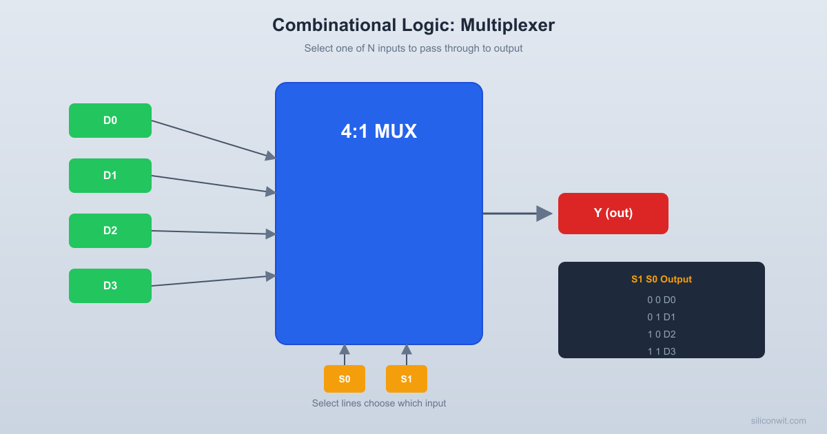
4-to-1 Multiplexer
A 4-to-1 mux has 4 data inputs, 2 select lines, and 1 output:
  4-to-1 Multiplexer Block Diagram
  D0 ──┐       │  D1 ──┤     ┌─────┐       ├─────┤     │  D2 ──┤     │ MUX ├──── Y (output)       │     │ 4:1 │  D3 ──┘     └──┬──┘                │           ┌────┴────┐           S1       S0         (select lines)
Y
0
0
0
1
1
0
1
1
Boolean expression:
Each term is a 3-input AND gate. The four AND outputs feed into a 4-input OR gate.
General Pattern
An -to-1 multiplexer needs select lines. Common sizes:
Multiplexer
Data Inputs
Select Lines
2-to-1
2
1
4-to-1
4
2
8-to-1
8
3
16-to-1
16
4
Where Multiplexers Appear in MCUs
Inside your microcontroller, multiplexers are everywhere:
GPIO alternate function selection: Each GPIO pin can serve multiple functions (UART TX, SPI MOSI, timer output). A multiplexer controlled by configuration register bits selects which function reaches the pin.
Clock source selection: The RCC module uses multiplexers to choose between HSI, HSE, and PLL as the system clock source.
ADC channel selection: When you select which analog channel to convert, you are programming a multiplexer.
Demultiplexers (DEMUX)
A demultiplexer does the opposite of a multiplexer: it takes one input and routes it to one of several outputs based on the select lines.
1-to-4 Demultiplexer
0
0
D
0
0
0
0
1
0
D
0
0
1
0
0
0
D
0
1
1
0
0
0
D
Where is the input data. Only one output is active at a time; the others are held at 0.
In embedded systems: DMA channel routing uses demultiplexer-like logic to direct data from one source to one of several destinations.
Decoders
Concept
A decoder converts a binary code into individual output lines. Only one output is active at a time. A decoder is essentially a demultiplexer with the data input permanently set to 1.
2-to-4 Decoder
2 input lines, 4 output lines. Exactly one output is high for each input combination.
0
0
1
0
0
0
0
1
0
1
0
0
1
0
0
0
1
0
1
1
0
0
0
1
Boolean expressions:
Each output is one AND gate. The decoder is four AND gates plus two inverters.
3-to-8 Decoder
3 input lines, 8 output lines. The 74HC138 is a classic 3-to-8 decoder IC.
Active Output
0
0
0
0
0
1
0
1
0
0
1
1
1
0
0
1
0
1
1
1
0
1
1
1
Address Decoding in Memory Systems
This is one of the most important applications of decoders. When a microcontroller accesses memory, the upper address bits pass through a decoder to determine which memory chip or peripheral responds:
  Address decoding with a 3-to-8 decoder
  Address Bus  A15 ──┐  A14 ──┤ 3-to-8  ├── Y0 → Flash CS  A13 ──┤ Decoder ├── Y1 → SRAM CS        │ (74138) ├── Y2 → Periph 1 CS        │         ├── Y3 → Periph 2 CS        │         ├── Y4 → (unused)        │         ├── Y5 → (unused)        │         ├── Y6 → (unused)        └─────────┴── Y7 → (unused)
  A12..A0 go directly to each device  (8 KB per device)
Address Range
Decoder Output
Device
0x0000-0x1FFF
Flash memory
0x2000-0x3FFF
SRAM
0x4000-0x5FFF
Peripheral block 1
0x6000-0x7FFF
Peripheral block 2
The three highest address bits (A15, A14, A13) select which device is enabled. The remaining 13 bits address locations within that device, giving each device an 8 KB address range.
Encoders
Concept
An encoder is the reverse of a decoder. It has multiple input lines (only one should be active at a time) and produces a binary code representing which input is active.
4-to-2 Priority Encoder
A priority encoder handles the case where multiple inputs might be active simultaneously by giving priority to the highest-numbered input.
Valid
0
0
0
0
X
X
0
0
0
0
1
0
0
1
0
0
1
X
0
1
1
0
1
X
X
1
0
1
1
X
X
X
1
1
1
The “X” entries mean “don’t care.” If is active, the output is 11 regardless of what , , or are doing.
In embedded systems: The NVIC (Nested Vectored Interrupt Controller) in ARM Cortex-M microcontrollers uses priority encoding to determine which interrupt to service when multiple interrupts are pending simultaneously.
Half Adder
Concept
A half adder adds two single-bit numbers and produces a sum and a carry:
A
B
Sum
Carry
0
0
0
0
0
1
1
0
1
0
1
0
1
1
0
1
Look at the truth tables:
Sum matches the XOR truth table:
Carry matches the AND truth table:
A half adder is just one XOR gate and one AND gate. It is called “half” because it cannot handle a carry input from a previous stage.
Full Adder
Concept
A full adder adds two bits plus a carry-in from the previous stage, producing a sum and a carry-out:
  Full Adder Block Diagram
      A       B      │       │      ▼       ▼    ┌───────────┐    │           │    │   Full    │◄── Cin (carry in)    │   Adder   │    │           │    └──┬─────┬──┘       │     │       ▼     ▼      Sum   Cout (carry out)
A
B
Sum
0
0
0
0
0
0
0
1
1
0
0
1
0
1
0
0
1
1
0
1
1
0
0
1
0
1
0
1
0
1
1
1
0
0
1
1
1
1
1
1
Boolean expressions:
A full adder is built from two half adders and one OR gate, or equivalently from two XOR gates, two AND gates, and one OR gate.
Ripple Carry Adder
Chain full adders together to add two -bit numbers. The carry-out of each stage connects to the carry-in of the next:
A3 B3 A2 B2 A1 B1 A0 B0
| | | | | | | |
[Full] [Full] [Full] [Full]
Adder 3 Adder 2 Adder 1 Adder 0
| | | |
C4←──Cout C3←──Cout C2←──Cout C1←──Cout←── C0 (0)
| | | |
S3 S2 S1 S0
The 4-bit ripple carry adder adds two 4-bit numbers (A3..A0 + B3..B0) and produces a 4-bit sum (S3..S0) plus a carry-out (C4).
The “ripple” refers to how the carry propagates through each stage sequentially. The worst case delay is for the carry to ripple from the least significant bit to the most significant bit. This is simple but slow for large numbers. Modern CPUs use carry-lookahead adders for faster addition.
  4-bit ripple carry adder
  A3 B3    A2 B2    A1 B1    A0 B0   │  │     │  │     │  │     │  │  ┌┴──┴┐   ┌┴──┴┐   ┌┴──┴┐   ┌┴──┴┐  │ FA │◄──│ FA │◄──│ FA │◄──│ FA │◄── 0  │  3 │C3 │  2 │C2 │  1 │C1 │  0 │   Cin  └─┬──┘   └─┬──┘   └─┬──┘   └─┬──┘  C4│  S3    │  S2    │  S1    │  S0    ▼        ▼        ▼        ▼ (overflow)
Practical: Build a 4-to-1 Multiplexer from Gates
Parts Needed
Component
Quantity
74HC08 (quad AND)
2
74HC32 (quad OR)
1
74HC04 (hex inverter)
1
LEDs
1
220 ohm resistors
1
DIP switches (4-position)
1
Push buttons
2
Breadboard, jumper wires, 5V supply
1 set
Circuit Description
Set up four data inputs ( through ) using four DIP switch positions. Each switch connects to 5V (logic 1) or is pulled to GND (logic 0) through a 10K resistor.
Set up two select inputs (, ) using two push buttons with pull-down resistors.
Build the inverters: Use the 74HC04 to generate and from the select inputs.
Build four AND gates (3-input each): Each AND gate enables one data input based on the select combination.
Gate for : AND of , , . Use two 2-input AND gates cascaded (AND the first two, then AND the result with ).
Gate for : AND of , , .
Gate for : AND of , , .
Gate for : AND of , , .
OR the four AND outputs together using two stages of 74HC32 (OR the first two, OR the second two, then OR the results).
Connect the final OR output to an LED through a 220 ohm resistor.
Test: Set the DIP switches to different patterns and use the push buttons to select which input appears at the output. For example, set , , , . With , , the LED should light (selecting ). With , , the LED should be off (selecting ).
Practical: Build a 2-Bit Adder
Parts Needed
Component
Quantity
74HC86 (quad XOR)
1
74HC08 (quad AND)
1
74HC32 (quad OR)
1
LEDs
3
220 ohm resistors
3
DIP switches (4-position)
1
Breadboard, jumper wires, 5V supply
1 set
Building Two Full Adders
Assign DIP switches: SW1 = , SW2 = , SW3 = , SW4 = . Each switch connects to 5V when on and has a 10K pull-down to GND when off.
Build Full Adder 0 (LSB):
XOR gate 1: (use 74HC86, gate 1)
XOR gate 2: = . Since for the first adder, the sum is just . Connect this to the LED.
AND gate 1: (carry out for this stage). Use 74HC08, gate 1.
Build Full Adder 1 (MSB):
XOR gate 3: (use 74HC86, gate 2)
XOR gate 4: (use 74HC86, gate 3, where is the carry from Full Adder 0). This is . Connect to the LED.
For : AND gate 2 for , AND gate 3 for , OR gate for the two AND results. Connect to the LED.
Test all combinations using the truth table below. Verify each combination by checking the LED pattern.
Expected Sum ()
00 (0)
00 (0)
000 (0)
01 (1)
01 (1)
010 (2)
10 (2)
01 (1)
011 (3)
11 (3)
01 (1)
100 (4)
11 (3)
11 (3)
110 (6)
Exercises
Exercise 1: Design a 2-to-4 Decoder
Write the Boolean expressions for all four outputs of a 2-to-4 decoder. Then draw how you would build it using only 74HC04 (NOT) and 74HC08 (AND) ICs, listing which pins you would use.
Solution
Use 74HC04 gates 1 and 2 to create and . Then use all four AND gates from one 74HC08: gate 1 for , gate 2 for , gate 3 for , gate 4 for .
Exercise 2: 8-to-1 Multiplexer
How many select lines does an 8-to-1 multiplexer need? Write the Boolean expression for the output in terms of through and select lines , , .
Solution
3 select lines ().
Each term is a 4-input AND gate. The eight AND outputs feed into an 8-input OR tree.
Exercise 3: Adder Overflow
What is the maximum sum a 4-bit ripple carry adder can produce? What happens if both inputs are 1111 (15)?
Solution
The maximum 4-bit sum is . In binary: with . The full result is 5 bits: . The carry-out serves as the fifth bit. If you only look at the 4-bit sum (1110 = 14), you get the wrong answer. This is what “overflow” means: the result does not fit in the output width.
How This Connects to Embedded Programming
Address Decoding
When your MCU accesses address 0x40021000, internal decoders determine that this address maps to the RCC peripheral. The upper address bits pass through decoder logic that enables the correct peripheral block and disables all others.
GPIO Alternate Functions
Each GPIO pin has a multiplexer that selects between regular GPIO, UART, SPI, I2C, timer, and other functions. When you call GPIO_PinAFConfig() or set alternate function bits, you are programming this multiplexer.
The ALU Inside Your MCU
The Arithmetic Logic Unit that executes your +, -, &, |, ^ operations is built from adders, multiplexers, and logic gates exactly like the ones in this lesson, just 32 bits wide and with carry-lookahead for speed.
Interrupt Priority
The NVIC uses priority encoding to decide which interrupt to service. When multiple interrupts fire simultaneously, priority encoder logic selects the highest-priority pending interrupt, similar to the priority encoder discussed earlier.
Summary
Circuit
Function
Key Application
Multiplexer
Select one of N inputs
Clock source selection, GPIO mux
Demultiplexer
Route one input to one of N outputs
DMA routing, data distribution
Decoder
Binary code to individual lines
Address decoding, chip select
Encoder
Individual lines to binary code
Interrupt priority, keyboard scanning
Half adder
Add two bits
Building block for full adder
Full adder
Add two bits plus carry
ALU arithmetic, ripple carry chains
In the next lesson, you will add memory to your circuits. Flip-flops and latches store state, turning combinational logic into sequential circuits that can remember, count, and shift data.
Comments