This lesson brings together motor control and inertial sensing on a single PCB. You will design a “hat” board that plugs into any MCU dev board through pin headers, combining a DRV8833 dual H-bridge motor driver with an MPU6050 6-axis IMU. The challenge is routing high-current motor traces alongside sensitive analog signals without one corrupting the other. #KiCad #MotorDriver #IMU
Power and Signal Zone Separation
──────────────────────────────────────────
┌──────────────────────────────────────┐
│ MOTOR POWER ZONE │
│ ┌─────────┐ VMOT ──► screw term │
│ │ DRV8833 │ OUT1A ──► Motor 1 │
│ │ H-bridge│ OUT1B ──► Motor 1 │
│ └─────────┘ OUT2A ──► Motor 2 │
│ TVS diode OUT2B ──► Motor 2 │
│ wide traces (1A+) │
├─ ─ ─ ─ ─ ─ ─ ─ ─ ─ ─ ─ ─ ─ ─ ─ ─ ┤
│ GND split / gap (separation zone) │
├─ ─ ─ ─ ─ ─ ─ ─ ─ ─ ─ ─ ─ ─ ─ ─ ─ ┤
│ ANALOG/SENSOR ZONE │
│ ┌─────────┐ SDA ──┐ │
│ │ MPU6050 │ SCL ──┤ thin traces │
│ │ IMU │ │ to MCU │
│ └─────────┘ 3.3V LDO (clean) │
└──────────────────────────────────────┘
What We Are Building
Motor Driver and Sensor Integration Board
A compact expansion board that stacks onto any MCU dev board via 2x10 pin headers. It drives two DC motors (or one stepper) through a DRV8833 H-bridge, reads motion data from an MPU6050 accelerometer/gyroscope over I2C, and measures motor current with low-side shunt resistors and an MCP6001 op-amp. Screw terminals provide secure motor and power connections. Reverse polarity protection and TVS clamping guard against motor noise and wiring mistakes.
When motor power and sensitive sensors share a board, noise coupling is the primary enemy. Motors generate large current transients, voltage spikes from inductive kickback, and electromagnetic interference from commutation. The MPU6050, meanwhile, measures acceleration in fractions of a g using tiny capacitive elements. Without careful layout, motor noise corrupts IMU readings and makes the data useless.
The solution is to treat the board as two separate domains that happen to share a PCB. The motor domain handles high current, tolerates noise, and needs wide traces. The signal domain handles millivolt-level analog signals, I2C communication, and needs clean power with minimal noise. These domains share a ground connection, but only at a single, carefully chosen point.
Key principles for this design:
Principle
Application on This Board
Physical separation
Motor driver and power on the left half, IMU on the right half
Star grounding
Motor GND and signal GND meet at one point near the bulk capacitor
Wide power traces
Motor traces 1 mm or wider (rated for 1.5A)
Short motor loops
Screw terminals placed close to DRV8833 to minimize loop area
Decoupling at every IC
100 nF ceramic caps within 3 mm of each power pin
Bulk capacitance
100 uF electrolytic on motor power input absorbs voltage spikes
Analog separation
Op-amp output filtered before reaching MCU analog input
DRV8833 Motor Driver
The DRV8833 from Texas Instruments is a dual H-bridge motor driver rated for 1.5A per channel (2A peak). It accepts a motor supply voltage from 2.7V to 10.8V, making it suitable for small DC motors and stepper motors commonly used in robotics. The IC comes in an HTSSOP-16 package with an exposed thermal pad on the bottom.
Pinout and Functionality
The DRV8833 provides two independent H-bridge channels, each controlled by two PWM input pins:
Pin
Function
Connection
AIN1, AIN2
Channel A PWM inputs
MCU PWM outputs
BIN1, BIN2
Channel B PWM inputs
MCU PWM outputs
AOUT1, AOUT2
Channel A motor outputs
Motor A screw terminal
BOUT1, BOUT2
Channel B motor outputs
Motor B screw terminal
VM
Motor supply voltage
External power (2.7V to 10.8V)
VCC
Logic supply
5V from MCU header
GND
Ground (multiple pins)
Ground plane
nSLEEP
Sleep control (active low)
Pull high through 10k for always-on, or connect to MCU GPIO
nFAULT
Fault output (open drain)
Pull high through 10k, connect to MCU GPIO
Exposed pad
Thermal pad
Solder to ground, thermal vias to back copper
Motor control modes: Each channel supports forward, reverse, brake, and coast by varying the logic levels on the two input pins. With PWM on one input and GND on the other, you get variable speed in one direction. Swapping which pin gets the PWM reverses the direction.
Thermal Management
The DRV8833 dissipates significant heat at full load. The RDS(on) of the internal MOSFETs is approximately 360 milliohms (high-side + low-side combined). At 1.5A continuous per channel, each channel dissipates roughly 0.81W. With both channels loaded, total dissipation reaches about 1.6W.
Solder the exposed pad to a large copper area on the top layer. The pad is the primary heat path out of the IC.
Place thermal vias in an array (3x3 or 4x4, 0.3mm drill) under the exposed pad. These carry heat from the top copper to the bottom layer.
Add a copper pour on the bottom layer directly under the DRV8833 footprint. This acts as a heat spreader and radiates heat to the surrounding air.
Connect the thermal pad to GND. The exposed pad is internally connected to ground inside the DRV8833, so the thermal copper pour also serves as part of the ground plane.
Sleep and Fault Pins
Pull the nSLEEP pin high through a 10 kohm resistor for always-on operation. If your MCU needs to disable the motor driver (for power saving or safety), route nSLEEP to a GPIO pin. When pulled low, the DRV8833 enters a low-power sleep mode drawing only a few microamps.
The nFAULT pin is an open-drain output that goes low when the driver detects an overcurrent or thermal shutdown condition. Pull it high through 10 kohm and connect to a MCU GPIO with interrupt capability. This lets your firmware detect and respond to motor faults.
MPU6050 IMU
The MPU6050 is a 6-axis inertial measurement unit combining a 3-axis accelerometer and a 3-axis gyroscope in a single QFN-24 package. It communicates over I2C at up to 400 kHz. The accelerometer measures from plus or minus 2g up to plus or minus 16g, while the gyroscope covers plus or minus 250 to plus or minus 2000 degrees per second. An internal digital motion processor (DMP) can offload sensor fusion from the main MCU.
I2C Interface
The MPU6050 uses a standard I2C interface with SDA and SCL lines. Pull-up resistors (10 kohm to 3.3V) are placed on the board near the IMU. The AD0 pin selects the I2C address: tie it to GND for address 0x68, or to VCC for 0x69. This lets you place two MPU6050s on the same bus if needed.
The INT pin provides a configurable interrupt output. Connect it to a MCU GPIO for data-ready notifications. This avoids polling and ensures you read the sensor at a consistent rate.
Placement Considerations
The MPU6050 is sensitive to mechanical vibration and board flex. On a robot or moving platform:
Place the MPU6050 near the center of the board to minimize the effect of board flex
Position it as close as possible to the center of rotation if the board mounts on a rotating platform
Keep the sensor away from the motor driver to reduce electromagnetic interference
Avoid placing it near the board edge where vibrations amplify
Use a solid ground plane under the MPU6050 for both electrical shielding and mechanical rigidity
Decoupling
The MPU6050 requires careful decoupling on two separate power pins:
VDD pin: 100 nF ceramic + 10 nF ceramic, placed within 2 mm of the pin
VLOGIC pin: 100 nF ceramic, close to the pin. VLOGIC sets the I2C logic level and is typically connected to 3.3V through the decoupling cap
Route the 3.3V supply to the MPU6050 through a dedicated trace from the LDO, not shared with motor power.
Current Sensing
Measuring motor current lets your firmware detect stall conditions, estimate torque, and protect the mechanical system from overload. This board uses low-side current sensing: a small shunt resistor sits between the motor driver ground return and the actual ground. The voltage across the shunt is proportional to the motor current.
Shunt Resistor Selection
The shunt resistors are 0.1 ohm in a 2512 package, rated for 1W. At the maximum motor current of 1.5A, the voltage drop and power dissipation are:
Parameter
Formula
Value
Voltage drop
V = I x R
1.5A x 0.1 ohm = 150 mV
Power dissipation
P = I^2 x R
(1.5)^2 x 0.1 = 0.225W
Package rating
1W (4.4x safety margin)
The 150 mV signal is too small for most MCU ADCs to resolve accurately (a 10-bit ADC at 3.3V reference has 3.2 mV per step, giving only ~47 steps across the full range). An op-amp amplifies this signal to a more useful level.
Op-Amp Amplifier
The MCP6001 is configured as a non-inverting amplifier with a gain of 10:
Parameter
Value
Configuration
Non-inverting
Feedback resistor (R_f)
9 kohm
Input resistor (R_in)
1 kohm
Gain
1 + (R_f / R_in) = 1 + 9 = 10
Output at 1.5A
150 mV x 10 = 1.5V
Output at 0.5A
50 mV x 10 = 0.5V
The MCP6001 is rail-to-rail on both input and output, operates from a single 3.3V or 5V supply, and has low offset voltage (under 3 mV typical). Place a 10 nF filter capacitor on the op-amp output to smooth out the PWM-frequency ripple before the signal reaches the MCU ADC pin.
One shunt and one op-amp channel measure the total current for both motor channels combined. If you need per-channel current sensing, duplicate the shunt and op-amp circuit for each channel.
Protection Circuits
Reverse Polarity Protection
A P-channel MOSFET (SI2301) on the motor power input prevents damage if the external supply is connected backwards. In normal operation, the MOSFET body diode conducts initially, then the gate voltage turns on the MOSFET fully, resulting in very low voltage drop (roughly 50 mV at 1.5A). If the polarity is reversed, the MOSFET stays off and blocks current.
Connect the source of the P-MOSFET to the positive terminal of the power input screw terminal.
Connect the drain to the VM net that feeds the DRV8833 and bulk capacitor.
Connect the gate to the ground side of the power input. When positive voltage is applied correctly, V_GS is negative (turning on the P-FET). When reversed, V_GS is zero or positive (keeping it off).
TVS Diode
A SMBJ12A transient voltage suppressor diode clamps voltage spikes on the motor power rail. Motor back-EMF and inductive switching can produce brief voltage spikes well above the nominal supply. The TVS diode conducts and clamps these spikes before they reach the DRV8833 (which has an absolute maximum of 11.8V on VM).
Place the TVS diode directly across the motor power input, after the reverse polarity MOSFET and before the DRV8833.
Flyback Diodes
The DRV8833 has internal free-wheeling diodes built into its H-bridge MOSFETs. External flyback diodes (SS14 Schottky) across each motor terminal are optional but provide extra protection. They clamp inductive kickback faster than the internal diodes and reduce stress on the driver IC. Place them close to the screw terminals, with cathode to positive motor terminal and anode to negative.
Bulk Capacitor
A 100 uF electrolytic capacitor on the motor power input serves as a local energy reservoir. When motors start or reverse direction, they draw large current transients. The bulk capacitor supplies this transient current locally, preventing the voltage from drooping at the DRV8833 VM pin. Place it as close to the DRV8833 as possible, with short, wide traces.
Schematic Capture in KiCad
Organize the schematic into clearly labeled sections. KiCad 9 supports hierarchical sheets, but for a board this simple, a single sheet with grouped sections works well.
Motor driver section. Place the DRV8833 symbol at the center-left of the sheet. Connect VM to the protected power rail through the bulk capacitor. Connect VCC to 5V from the MCU header. Add 100 nF decoupling caps on both VM and VCC, placed close to the symbol. Route AIN1, AIN2, BIN1, BIN2 to the MCU header pins labeled PWM1 through PWM4. Route AOUT1/AOUT2 to screw terminal J2 and BOUT1/BOUT2 to screw terminal J3.
IMU section. Place the MPU6050 on the right side of the sheet. Connect VDD and VLOGIC to the 3.3V LDO output through their respective decoupling networks. Route SDA and SCL to the MCU header I2C pins through 10 kohm pull-ups. Connect AD0 to GND (address 0x68). Route INT to a MCU header GPIO pin.
Current sensing section. Place the shunt resistors (R1, R2) in series between the DRV8833 GND pins and the ground plane. Connect the junction between the shunts and the DRV8833 to the non-inverting input of the MCP6001. Add the gain resistors (R7, R8) and filter cap (C8). Route the op-amp output to an analog input pin on the MCU header.
Protection section. Place the P-MOSFET (Q1) between J4 (power input screw terminal) and the VM net. Place the TVS diode (D1) across the VM net and GND, after Q1. Place flyback diodes (D2 through D5) across the motor screw terminals.
MCU header section. Place the 2x10 pin header (J1) and assign pins logically.
Run ERC. Fix any unconnected pins, missing power flags, or conflicting net names. Assign footprints to all symbols: HTSSOP-16 for DRV8833, QFN-24 for MPU6050, SOT-23-5 for MCP6001, SOT-223 for AMS1117-3.3, 2512 for shunt resistors, SMA for diodes, 5.08mm pitch for screw terminals.
MCU header pin assignments:
Pin
Function
Direction
1
5V
Power in (from MCU)
2
GND
Ground
3
PWM1 (AIN1)
Input to DRV8833
4
PWM2 (AIN2)
Input to DRV8833
5
PWM3 (BIN1)
Input to DRV8833
6
PWM4 (BIN2)
Input to DRV8833
7
SDA (I2C)
Bidirectional, MPU6050
8
SCL (I2C)
Output to MPU6050
9
INT (MPU6050)
Interrupt output
10
nFAULT
Fault output from DRV8833
11
nSLEEP
Sleep control to DRV8833
12
ISENSE
Analog, current sense output
13-18
Reserved
Spare GPIO
19
3.3V
Power out (from on-board LDO)
20
GND
Ground
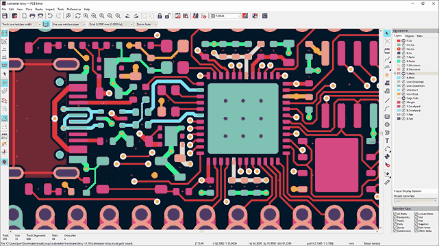
PCB Layout
The PCB layout is where mixed-signal design principles turn into copper. This is a 2-layer board, so you do not have dedicated inner planes. Instead, you rely on careful copper pours, physical separation, and trace width management to keep motor noise away from the IMU.
Board Outline and Zones
Set the board outline to 50 x 45 mm. Place M3 mounting holes (3.2 mm drill) at each corner, inset 3 mm from the edges. These allow standoff mounting above the MCU dev board.
Divide the board conceptually into two halves. The left half is the power domain: DRV8833, screw terminals, bulk capacitor, protection circuits, shunt resistors. The right half is the signal domain: MPU6050, LDO, I2C pull-ups.
Place the MCU header along the bottom edge, spanning both domains. This is where signals cross from one domain to the other, and where the star ground connection point sits.
Component Placement
Component
Placement
Rationale
DRV8833 (U1)
Center-left
Close to screw terminals, away from IMU
Screw terminals (J2, J3, J4)
Left edge
Easy access, short motor traces
Bulk cap (C1)
Next to DRV8833
Minimize loop area for transient current
TVS diode (D1)
Near J4
Clamp spikes at the source
P-MOSFET (Q1)
Between J4 and C1
First component in the power path
Shunt resistors (R1, R2)
Below DRV8833
In the ground return path
MCP6001 (U3)
Between DRV8833 and MPU6050
Close to shunts, output routed to header
MPU6050 (U2)
Center-right
Away from motor traces and screw terminals
AMS1117-3.3 (U4)
Near MPU6050
Clean 3.3V supply, short trace to IMU
MCU header (J1)
Bottom edge
Stacks onto dev board below
Trace Width and Routing
Motor current traces must be wide enough to carry 1.5A without excessive heating. For a 1 oz copper 2-layer board:
Trace Type
Width
Current
Notes
Motor power (VM)
1.5 mm
Up to 3A (both channels)
Keep short, use copper pour where possible
Motor outputs
1.0 mm
Up to 1.5A per channel
DRV8833 to screw terminals
Ground return
1.0 mm or pour
Up to 3A
Use copper pour on bottom layer
I2C (SDA, SCL)
0.2 mm
< 1 mA
Keep away from motor traces
PWM signals
0.2 mm
< 1 mA
Route on opposite side from I2C
Analog (ISENSE)
0.2 mm
< 1 mA
Guard with ground traces on both sides
Thermal Via Array
Under the DRV8833 exposed pad, place a grid of thermal vias:
Via drill: 0.3 mm
Via pad: 0.6 mm
Array: 4 x 4 (16 vias) within the exposed pad area
Connection: All vias connect to a copper pour on the bottom layer
Solder mask: Tent the vias on the bottom side to prevent solder wicking during reflow
Ground Plane Strategy
On a 2-layer board, you cannot have a complete ground plane without interrupting signal routing. The approach:
Fill the bottom layer with a ground pour. This acts as your primary ground plane and heat spreader.
Split the ground pour conceptually into motor ground (left half) and signal ground (right half). Do not physically cut the pour. Instead, route motor return current through the left side and signal return current through the right side by placement.
Connect both ground domains at a single point near the bulk capacitor and MCU header GND pins. This is the star ground point. Motor current return flows through the left side of the pour, through the star point, and out through the MCU header GND. Signal current takes the right side.
Add ground vias liberally around the MPU6050 and between the motor and signal domains. These stitch the top and bottom ground pours together, reducing impedance and improving shielding.
Top layer ground pour: Fill remaining top layer space with ground copper, especially around the MPU6050. This provides additional shielding from motor noise radiating across the board surface.
Design Rule Check
Before generating manufacturing files, run the DRC in KiCad:
Minimum trace width: 0.15 mm (for signal traces)
Minimum clearance: 0.15 mm
Minimum via drill: 0.3 mm
Thermal relief on all pads connecting to copper pours
No unrouted nets
No overlapping pads or silk
Manufacturing
Export Gerber files and drill files from KiCad using the same process as previous lessons. For fabrication through JLCPCB or similar services:
Parameter
Setting
Layers
2
Dimensions
50 x 45 mm
PCB thickness
1.6 mm
Copper weight
1 oz (consider 2 oz for better current handling)
Surface finish
HASL (lead-free) or ENIG
Solder mask
Green (or any color)
Minimum trace/space
6/6 mil
If you choose 2 oz copper, you can use narrower traces for the same current capacity. A 0.75 mm trace at 2 oz copper carries roughly the same current as a 1.5 mm trace at 1 oz.
Assembly Notes
Solder the QFN/LGA components first. The DRV8833 (HTSSOP-16 with exposed pad) and MPU6050 (QFN-24) require reflow soldering. Apply solder paste with a stencil and reflow in a hot air station or reflow oven. The DRV8833 exposed pad needs adequate solder paste to make thermal contact.
Solder the small SMD passives next. Capacitors, resistors, and the SOT-23-5 op-amp can be hand soldered or reflowed together with the ICs.
Solder the SOT-223 LDO. The AMS1117-3.3 has a large tab that needs a good solder joint to the PCB for thermal dissipation.
Install the through-hole components last. Screw terminals and pin headers are soldered from the bottom side. Solder the pin headers with the board plugged into a breadboard or the target MCU board to ensure alignment.
Test without motors. Power the board through the MCU header (5V and GND). Verify 3.3V LDO output. Check that the DRV8833 is not in sleep mode (nSLEEP should be high). Send PWM signals and verify them on the motor output terminals with an oscilloscope or logic analyzer before connecting actual motors.
Connect motors and test. Attach motors to the screw terminals. Start with low PWM duty cycle and gradually increase. Monitor the current sense output on the analog pin. Check the MPU6050 is responding on I2C (scan for address 0x68).
Firmware: Motor Control with IMU Feedback
The following Arduino sketch demonstrates the core functionality of this board. It initializes the MPU6050 over I2C, reads accelerometer data, and uses a simple proportional controller to drive the motors based on board tilt. It also reads the current sense voltage through the ADC and prints all data to the serial monitor.
This sketch works with any Arduino-compatible MCU (Arduino Uno, Nano, ESP32, STM32 with Arduino core, etc.). Adjust the pin definitions to match your MCU header wiring.
// Motor Driver + IMU Integration Board - Basic Control Sketch
// Drives two DC motors proportionally to board tilt using MPU6050 data
#include<Wire.h>
// Pin definitions (match MCU header assignments)
constint PWM1_PIN =3; // AIN1 - Motor A forward
constint PWM2_PIN =5; // AIN2 - Motor A reverse
constint PWM3_PIN =6; // BIN1 - Motor B forward
constint PWM4_PIN =9; // BIN2 - Motor B reverse
constint ISENSE_PIN = A0; // Current sense analog input
Comments