The real world is analog: light intensity, temperature, force, and sound are all continuous signals. The ADC (Analog-to-Digital Converter) on the ATmega328P samples these signals and converts them into 10-bit digital values your firmware can process. In this lesson you will configure the ADC registers directly, explore reference voltage options, compare single-conversion and free-running modes, and implement oversampling for noise reduction. The project uses two photoresistors (LDRs) to detect which direction is brighter, displaying a live bar graph on the OLED that shows the relative light level from each sensor. #ADC #AnalogSignals #Photoresistor
What We Are Building
Light-Tracking Indicator
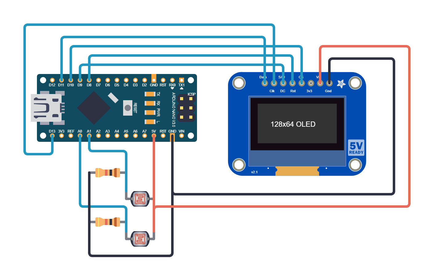
Two LDRs (light-dependent resistors) are mounted side by side in voltage divider circuits, each feeding a separate ADC channel. The firmware samples both channels, computes a 16-sample running average for noise reduction, and renders two horizontal bar graphs on the OLED display. A directional arrow in the center indicates which side is brighter. The system updates at approximately 20 Hz, giving a smooth, responsive display.
Project specifications:
Parameter
Value
MCU
ATmega328P (on Arduino Nano or Uno)
ADC channels
ADC0 (PC0) and ADC1 (PC1)
Resolution
10-bit (0 to 1023)
Reference
AVcc (5V)
ADC clock
125 kHz (prescaler 128)
Oversampling
16 samples averaged per reading
Display
SSD1306 128x64 OLED (SPI)
Update rate
~20 Hz
Parts for This Lesson
Ref
Component
Quantity
Notes
1
Arduino Nano or Uno (ATmega328P)
1
From previous lessons
2
Breadboard
1
From previous lessons
3
LDR (photoresistor)
2
5mm, typical 10K in daylight
4
10K ohm resistor
2
Voltage divider partners
5
SSD1306 OLED 128x64 (SPI)
1
From Lesson 6
6
Jumper wires
~6
Male-to-male
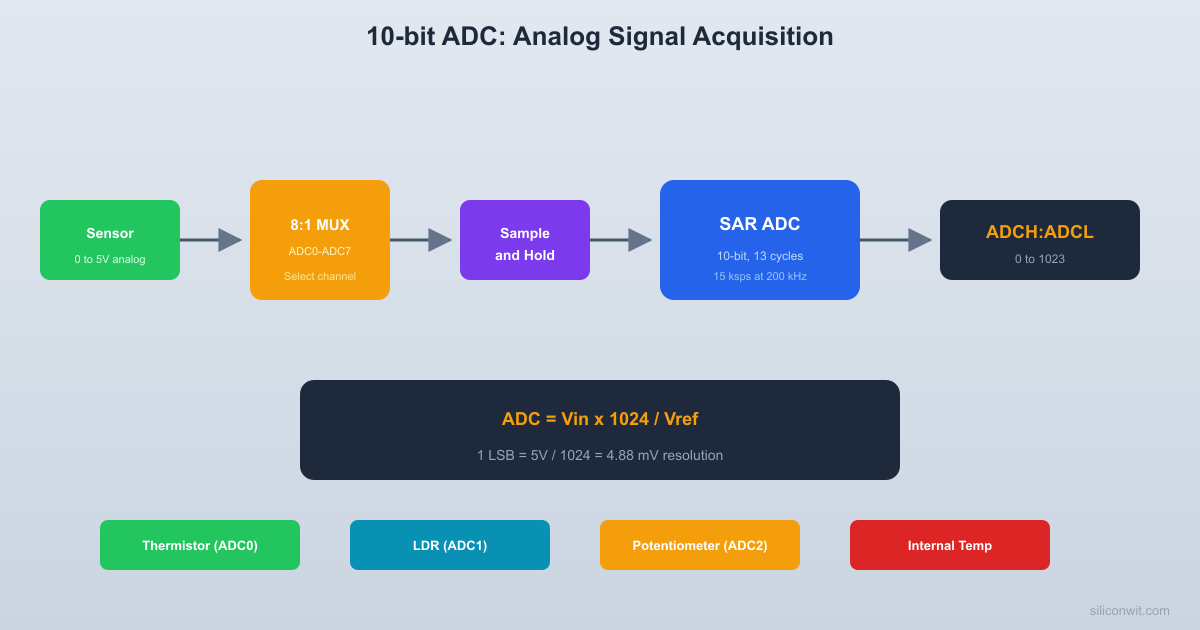
ADC Register Overview
The ATmega328P ADC converts an analog voltage to a 10-bit digital value using successive approximation. The input multiplexer selects which pin feeds the converter, and the prescaler generates a suitable ADC clock from the system clock.
  ATmega328P ADC block diagram:
  ADC0 (PC0) --+  ADC1 (PC1) --+    +--------+   +----------+  ADC2 (PC2) --+--->|  MUX   |-->|   S/H    |  ADC3 (PC3) --+    | (ADMUX)|   | (sample  |  ADC4 (PC4) --+    +--------+   |  & hold) |  ADC5 (PC5) --+        |        +----+-----+  Temp sensor--+     channel          |  1.1V ref  ---+     select           v                              +---------------+  AVCC --+--> Reference -+--->|  10-bit SAR   |  AREF --+    select     |   |  Converter    |  1.1V --+   (REFS1:0)   |   +-------+-------+                          |           |  F_CPU --> Prescaler ----+     +-----+-----+            (ADPS2:0)     |     | ADCL/ADCH |            /128=125kHz   |     | (result)  |                          |     +-----------+                          |                     ADC clock
The ATmega328P ADC is a successive-approximation converter with 10-bit resolution. It has 8 multiplexed input channels (ADC0 through ADC7, though ADC6 and ADC7 are only available on surface-mount packages). Three registers control the ADC: ADMUX selects the reference voltage and input channel, ADCSRA controls the enable, start, prescaler, and interrupt, and ADCSRB selects the trigger source for auto-trigger mode.
The ADC needs a clock between 50 kHz and 200 kHz for full 10-bit resolution. With a 16 MHz system clock, prescaler 128 gives 125 kHz, which is in the optimal range. A single conversion takes 13 ADC clock cycles (25 for the first conversion after enabling), so each reading takes about 104 microseconds.
/* First conversion (25 clock cycles, discard result) */
ADCSRA |= (1<< ADSC);
while (ADCSRA & (1<< ADSC));
}
staticuint16_tadc_read(uint8_tchannel)
{
/* Select channel (clear old, set new) */
ADMUX = (ADMUX &0xF0) | (channel &0x0F);
/* Start conversion */
ADCSRA |= (1<< ADSC);
while (ADCSRA & (1<< ADSC));
return ADC; /* Read 10-bit result */
}
Free-Running Mode
In free-running mode, the ADC starts a new conversion automatically as soon as the previous one finishes. This is useful when you need continuous sampling at the maximum rate. You enable it by setting ADATE (auto-trigger enable) in ADCSRA and selecting free-running as the trigger source in ADCSRB (ADTS2:0 = 000).
staticvoidadc_init_freerun(uint8_tchannel)
{
ADMUX = (1<< REFS0) | (channel &0x0F);
ADCSRA = (1<< ADEN) | (1<< ADSC) | (1<< ADATE)
| (1<< ADPS2) | (1<< ADPS1) | (1<< ADPS0);
ADCSRB =0; /* Free-running trigger source */
}
/* Read the latest result (non-blocking) */
staticuint16_tadc_read_freerun(void)
{
return ADC;
}
Oversampling for Noise Reduction
Averaging reduces noise by canceling out random fluctuations. Each individual sample has noise, but the mean of 16 samples is much closer to the true value.
  Effect of oversampling (16 samples):
  Raw samples (noisy):  512 508 515 510 513 507 514 511  509 516 510 512 508 513 511 510
  Average: 512 (clean)
  Noise reduction = sqrt(N) = sqrt(16) = 4x  Effective resolution gain: ~2 bits
ADC readings are noisy, especially on a breadboard with long wires and a switching USB power supply. Averaging multiple samples reduces random noise by the square root of the number of samples. Sixteen samples averaged together reduce noise by a factor of 4 (roughly 2 extra bits of effective resolution). The trade-off is slower update rate, but at 125 kHz ADC clock, 16 conversions still complete in under 2 milliseconds.
#defineOVERSAMPLE_COUNT16
staticuint16_tadc_read_averaged(uint8_tchannel)
{
uint32_t sum =0;
for (uint8_t i =0; i < OVERSAMPLE_COUNT; i++) {
sum +=adc_read(channel);
}
return (uint16_t)(sum / OVERSAMPLE_COUNT);
}
LDR Voltage Divider Circuit
Each LDR forms a voltage divider with a fixed 10K resistor.
  Dual LDR circuit:
       VCC            VCC        |              |      [LDR]          [LDR]      Left           Right        |              |  PC0 --+         PC1--+  (ADC0) |        (ADC1)|        |              |      [10K]          [10K]        |              |       GND            GND
  Bright light: LDR low R, high V at ADC  Darkness:     LDR high R, low V at ADC
The LDR connects from the ADC pin to VCC, and the 10K resistor connects from the ADC pin to ground. This is a standard voltage divider configuration. In bright light, the LDR resistance drops (to around 1K or less), and the voltage at the ADC pin rises toward VCC. In darkness, the LDR resistance increases (to hundreds of kilohms), and the voltage drops toward ground.
Signal
Arduino Pin
ATmega328P Pin
Connection
LDR Left
A0
PC0 (ADC0)
LDR to VCC, 10K to GND
LDR Right
A1
PC1 (ADC1)
LDR to VCC, 10K to GND
ADC Value to Voltage Conversion
V = (ADC_value / 1023.0) * V_ref
For AVcc reference (5V): an ADC reading of 512 corresponds to approximately 2.5V.
Complete Firmware
#defineF_CPU16000000UL
#include<avr/io.h>
#include<util/delay.h>
#include<string.h>
/* From Lesson 6: spi_init(), oled_init(), oled_flush(),
elseif (diff <-50) dir ='>'; /* Right is brighter */
fb_draw_arrow(60, 6, dir);
/* Numeric values */
charbuf[5];
utoa(left, buf, 10);
fb_draw_string(30, 0, buf);
utoa(right, buf, 10);
fb_draw_string(70, 0, buf);
oled_flush();
_delay_ms(50); /* ~20 Hz update */
}
}
ADC Noise Reduction Sleep Mode
The ATmega328P has a dedicated ADC Noise Reduction sleep mode. When entered, the CPU halts and most digital circuitry stops switching, which significantly reduces noise coupled into the ADC. The ADC continues to operate and triggers an interrupt when the conversion completes, waking the CPU. This is useful when you need the best possible accuracy from the 10-bit converter.
#include<avr/sleep.h>
#include<avr/interrupt.h>
ISR(ADC_vect)
{
/* Conversion complete, CPU wakes up */
}
staticuint16_tadc_read_quiet(uint8_tchannel)
{
ADMUX = (ADMUX &0xF0) | (channel &0x0F);
ADCSRA |= (1<< ADIE); /* Enable ADC interrupt */
set_sleep_mode(SLEEP_MODE_ADC);
sei();
sleep_mode(); /* Enter sleep, ADC starts automatically */
ADCSRA &=~(1<< ADIE); /* Disable ADC interrupt */
return ADC;
}
Exercises
Add a third LDR and display three bar graphs. Use channels ADC0, ADC1, and ADC2.
Implement oversampling with decimation to get 12-bit effective resolution. Take 256 samples, sum them (result fits in uint32_t), then right-shift by 4 to get a 12-bit value (0 to 4095).
Stream the raw ADC values over UART (from Lesson 5) at 100 Hz and plot them in real time using a serial plotter or Python script. Observe the noise with and without averaging.
Implement a simple peak detector: track and display the maximum ADC reading seen since the last reset (button press clears the peak).
Summary
You now understand the ATmega328P ADC at the register level: reference voltage selection, channel multiplexing, prescaler configuration, single-conversion and free-running modes, and the noise reduction sleep mode. Oversampling with averaging is a practical technique that improves effective resolution with minimal code. The light-tracking indicator demonstrates real-time analog signal acquisition with visual feedback, a pattern that applies to any analog sensor interfacing.
Comments