In this lesson you will design a complete STM32F103C8T6 development board in the classic Blue Pill form factor. The board includes USB for programming and serial communication, an SWD debug header, dual crystal oscillators, 3.3V regulation, and all GPIO broken out to pin headers. More importantly, this is your first professional fab house order: you will generate Gerber, BOM, and pick-and-place files, then walk through the entire JLCPCB ordering process. #KiCad #STM32 #PCBDesign
  Decoupling Capacitor Placement  ──────────────────────────────────────────       100nF      100nF      100nF        │           │           │  VDD──┤───VDD────┤───VDD────┤───VDD        │           │           │  ┌─────┴───────────┴───────────┴─────┐  │     STM32F103C8T6                  │  │  Pin 24   Pin 36   Pin 48         │  │  (VDD)    (VDD)    (VDD)          │  └────────────────────────────────────┘        │           │           │  GND──┘───GND────┘───GND────┘───GND
  Place each 100nF cap as close as  possible to its VDD/GND pin pair.  Short, wide traces to ground plane.
What We Are Building
STM32 Blue Pill Development Board
A Blue Pill style development board built around the STM32F103C8T6 (ARM Cortex-M3, 72 MHz). The board provides USB connectivity for programming via the built-in bootloader, an SWD header for debugging, and two rows of pin headers exposing every GPIO pin. Power comes from USB 5V, regulated down to 3.3V by an AMS1117-3.3 LDO. This is the board you will send to JLCPCB for professional fabrication and partial assembly.
Board specifications:
Parameter
Value
MCU
STM32F103C8T6 (LQFP-48, 0.5mm pitch)
Core
ARM Cortex-M3, 72 MHz max
Memory
64 KB Flash, 20 KB SRAM
HSE Crystal
8 MHz (for PLL to 72 MHz)
LSE Crystal
32.768 kHz (for RTC)
USB
Type-B Mini, full-speed (12 Mbps)
Power
AMS1117-3.3 LDO from USB 5V
Debug
4-pin SWD header (SWDIO, SWCLK, GND, 3V3)
Boot
Boot0/Boot1 jumpers
GPIO
2x 20-pin headers (all GPIO broken out)
LEDs
User LED on PC13, power LED
Board size
55 x 25 mm (Blue Pill form factor)
Bill of Materials
Ref
Component
Package
Qty
Notes
U1
STM32F103C8T6
LQFP-48
1
0.5mm pitch
U2
AMS1117-3.3
SOT-223
1
3.3V LDO
Y1
8 MHz
HC49/SMD or 3.2x2.5mm
1
HSE crystal
Y2
32.768 kHz
2x1.2mm SMD
1
LSE crystal (RTC)
  Gerber File Set for JLCPCB  ──────────────────────────────────────────  project-F_Cu.gtl      Front copper  project-B_Cu.gbl      Back copper  project-F_Mask.gts    Front solder mask  project-B_Mask.gbs    Back solder mask  project-F_Silkscreen.gto  Front silkscreen  project-B_Silkscreen.gbo  Back silkscreen  project-Edge_Cuts.gm1     Board outline  project.drl               Drill file  project-PTH.drl           Plated holes  project-NPTH.drl          Non-plated holes
  Zip all files ──► Upload to JLCPCB  Also generate: BOM (.csv) + CPL (.csv)  for SMT assembly service.
Reference
Value
Package
Qty
Function
C1, C2
20 pF
0805
2
HSE load caps
C3, C4
6.8 pF
0805
2
LSE load caps
C5-C9
100 nF
0805
5
Decoupling (each VDD pin)
C10
4.7 µF
0805
1
Bulk decoupling
C11, C12
10 µF
0805
2
LDO input/output caps
C13
100 nF
0805
1
NRST filter cap
C14
1 µF
0805
1
VDDA decoupling
R1
1.5 kΩ
0805
1
USB D+ pull-up
R2
10 kΩ
0805
1
NRST pull-up
R3
100 kΩ
0805
1
Boot0 pull-down
R4, R5
330 Ω
0805
2
LED current limiting
D1
Green LED
0805
1
Power indicator
D2
Blue/Green LED
0805
1
User LED (PC13)
J1
USB Mini-B
SMD
1
Power + data
J2
1x4 pin header
2.54mm
1
SWD debug
J3, J4
1x20 pin header
2.54mm
2
GPIO breakout
JP1
1x3 pin header + jumper
2.54mm
1
Boot0 select
SW1
Tactile switch
SMD 3x6mm
1
Reset
STM32 Fundamentals
The STM32F103C8T6 is an ARM Cortex-M3 microcontroller from STMicroelectronics. It runs at up to 72 MHz, has 64 KB of flash and 20 KB of SRAM, and includes peripherals like USB, I2C, SPI, UART, ADC, and timers. The “C8” in the part number tells you: C = 48 pins, 8 = 64 KB flash. The “T6” means LQFP package, industrial temperature range.
Clock Tree
The STM32F103 has a flexible clock system:
HSI (High Speed Internal): 8 MHz RC oscillator, available without any external components. Less accurate than a crystal.
HSE (High Speed External): 4-16 MHz crystal input. We use 8 MHz, which the PLL multiplies by 9 to reach 72 MHz.
LSE (Low Speed External): 32.768 kHz crystal for the Real-Time Clock (RTC). This frequency divides evenly into 1 Hz for timekeeping.
PLL: Takes HSE or HSI as input and multiplies it. HSE 8 MHz x 9 = 72 MHz system clock.
Why STM32 Matters for PCB Designers
The STM32 family is one of the most widely used MCU families in professional products. Designing a board around it teaches you skills that transfer directly to commercial work: fine-pitch LQFP soldering, multi-rail power design, USB signal integrity, and proper decoupling for high-speed digital ICs. The Blue Pill form factor is compact enough to be challenging but simple enough for a third PCB project.
The STM32F103 runs on 3.3V. USB provides 5V, so we need a voltage regulator.
Place the USB Mini-B connector. Add USB_B_Mini from the Connector library. This provides VBUS (5V), D+, D-, and GND.
Place the AMS1117-3.3 LDO (SOT-223). Connect VBUS to the LDO input through a 10 µF input capacitor (C11). Connect the LDO output to a +3V3 power symbol through a 10 µF output capacitor (C12).
Add power symbols. Place +5V on the USB VBUS net, +3V3 on the LDO output, and GND throughout.
Wire the power path. USB VBUS to +5V, through C11 to LDO input, LDO output through C12 to +3V3. Keep the power LED (D1 + R4) connected from +3V3 to GND so it lights when 3.3V is present.
MCU and Decoupling
The STM32F103C8T6 in LQFP-48 has multiple VDD and VSS pins. Every VDD pin needs its own 100 nF decoupling capacitor placed as close to the pin as possible.
Place the STM32F103C8T6. Add STM32F103C8Tx from the MCU_ST_STM32F1 library. The LQFP-48 variant has pins on all four sides.
Connect power pins. Wire VDD (pins 24, 36, 48) and VDDA (pin 9) to +3V3. Wire VSS (pins 23, 35, 47) and VSSA (pin 8) to GND.
Add decoupling capacitors. Place 100 nF caps C5, C6, C7 on VDD pins 24, 36, and 48 respectively. Place C14 (1 µF) on VDDA (pin 9) for the analog supply. Place C10 (4.7 µF) as bulk decoupling near the MCU.
VBAT pin. Connect VBAT (pin 1) to +3V3. If you want battery backup for the RTC later, this is the pin you would connect to a coin cell instead.
HSE Crystal (8 MHz)
Place the 8 MHz crystal between OSC_IN (pin 5) and OSC_OUT (pin 6).
Add load capacitors. Place C1 (20 pF) from OSC_IN to GND and C2 (20 pF) from OSC_OUT to GND. The exact capacitor value depends on the crystal’s specified load capacitance (typically 10-20 pF). For a crystal with 20 pF load capacitance, use 33 pF caps (accounting for ~5 pF PCB stray capacitance). For a 10 pF load crystal, 20 pF caps work well.
No series resistors needed. The STM32F103 datasheet does not require external series resistors on the HSE pins for most crystals.
LSE Crystal (32.768 kHz)
Place the 32.768 kHz crystal between OSC32_IN (pin 3) and OSC32_OUT (pin 4).
Add load capacitors. Place C3 (6.8 pF) from OSC32_IN to GND and C4 (6.8 pF) from OSC32_OUT to GND. The 32.768 kHz crystal is sensitive; use the datasheet-recommended values.
Reset Circuit
NRST pin (pin 7). Connect a 100 nF capacitor (C13) from NRST to GND for noise filtering.
Pull-up resistor. Connect R2 (10 kΩ) from NRST to +3V3.
Reset button. Place an SMD tactile switch (SW1) from NRST to GND. Pressing it pulls NRST low and resets the MCU.
USB Circuit
The STM32F103 has a built-in USB full-speed (12 Mbps) peripheral. The USB data lines connect to PA11 (USB_DM / D-) and PA12 (USB_DP / D+).
Wire USB data lines. Connect the USB connector D- to PA11 and D+ to PA12.
D+ pull-up resistor. Place R1 (1.5 kΩ) from PA12 (D+) to +3V3. This pull-up tells the USB host that a full-speed device is connected. Without it, the host will not detect the board.
No external ESD protection is strictly required for a development board, but if you want to add it, place a USBLC6-2SC6 on the USB data lines.
SWD Debug Header
Place a 1x4 pin header (J2) for SWD. The four pins are: SWDIO (PA13), SWCLK (PA14), GND, and 3V3.
Wire SWDIO to PA13 (pin 34) and SWCLK to PA14 (pin 37). These pins default to SWD function after reset, so no remapping is needed.
Connect GND and 3V3 on the header. The 3V3 pin allows the debugger to sense the target voltage (and optionally power the board from the debugger).
Boot Configuration
The STM32F103 boot mode is selected by the Boot0 and Boot1 pins at reset:
Boot1
Boot0
Mode
X
0
Boot from flash (normal operation)
0
1
Boot from system memory (USB/UART bootloader)
1
1
Boot from SRAM
Boot0 jumper. Place a 1x3 pin header (JP1) with the center pin connected to Boot0 (pin 44). Connect one outer pin to GND (normal boot) and the other to +3V3 (bootloader mode). A jumper cap selects the mode. Add R3 (100 kΩ) from Boot0 to GND as a default pull-down so the board boots from flash even without the jumper.
Boot1. Tie Boot1 (pin 20, PB2) to GND with a direct connection. SRAM boot is rarely needed on a development board.
User LED and GPIO Headers
User LED. Connect D2 (LED) and R5 (330 Ω) in series from PC13 (pin 2) to +3V3. Note: on the STM32, GPIO pins sink current when set low, so the LED lights when PC13 outputs low.
GPIO headers. Place two 1x20 pin headers (J3 and J4) on opposite sides of the board. Map all remaining GPIO pins to these headers in a logical order, matching the Blue Pill pinout as closely as possible. Include +3V3, +5V, and GND pins on the headers.
Run ERC. Fix all errors and warnings before proceeding.
Board outline. On the Edge.Cuts layer, draw a 55 x 25 mm rectangle. This is the classic Blue Pill form factor, a narrow board designed to straddle a breadboard.
Layer setup. This is a 2-layer board: F.Cu and B.Cu. Verify in Board Setup > Board Stackup > Physical Stackup that you have two copper layers with 1.6mm FR-4 substrate.
Design rules for JLCPCB. Set the following minimums in Board Setup > Design Rules:
Minimum track width: 0.15 mm
Minimum clearance: 0.15 mm
Minimum via drill: 0.3 mm
Minimum via diameter: 0.6 mm
Default track width: 0.25 mm (signal), 0.4 mm (power)
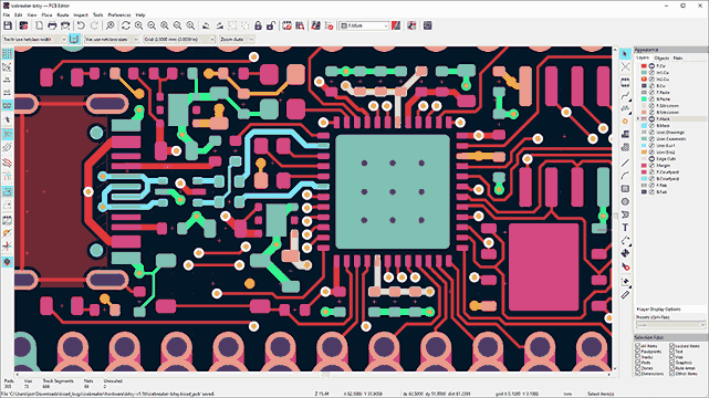
Component Placement
Update PCB from schematic (F8). All components appear in a cluster.
USB connector at the top edge, centered on the narrow side, plug facing outward.
LDO (U2) close to the USB connector with C11 and C12 immediately adjacent to its input and output pins. The LDO thermal pad should connect to a ground pour for heat dissipation.
MCU (U1) in the center of the board. Rotate it so that the USB data pins (PA11, PA12) face the USB connector, keeping those traces short.
8 MHz crystal (Y1) within 5 mm of OSC_IN/OSC_OUT pins, with C1 and C2 right next to it.
32.768 kHz crystal (Y2) within 3 mm of the OSC32 pins. This crystal is more sensitive to parasitic capacitance than the 8 MHz one. Place C3 and C4 adjacent.
Decoupling capacitors (C5-C9) each within 2 mm of its corresponding VDD pin. This is not optional; moving them farther away degrades power integrity at 72 MHz.
GPIO headers (J3, J4) along the long edges of the board, 2.54mm pitch, one row on each side. This is the signature Blue Pill layout.
SWD header (J2) at the bottom edge of the board.
Boot0 jumper (JP1) and reset button (SW1) on the top side, accessible but out of the way.
Routing
USB traces first. Route D+ and D- from the USB connector to PA11/PA12. Keep these traces short (under 25 mm), matched in length (within 2 mm of each other), and on the same layer. Use 0.3 mm width for the data lines. Avoid vias on USB data traces.
Crystal traces. Route HSE and LSE crystal traces as short as possible. Do not route any other signals between the crystal and the MCU pins. Keep digital signals away from the crystal area.
Power traces. Route +3V3 and +5V using 0.4 mm traces. The main power path from USB through the LDO should be direct and short.
Decoupling capacitor traces. Route each 100 nF cap directly to its VDD pin and to the nearest GND via. The loop area (VDD pin, trace to cap, cap, trace to GND via) should be as small as possible.
GPIO to headers. Route the remaining GPIO pins to the edge headers. These are low-speed signals, so routing is straightforward. Use 0.25 mm traces.
Ground pour. Add a GND copper zone on both F.Cu and B.Cu. Fill with B (Build All Zones). The ground pour on the back layer acts as a ground plane, improving signal integrity and providing a return path for high-frequency currents.
Add stitching vias. Place GND vias around the board perimeter and between the two ground pours. This ties the front and back ground planes together. Add extra stitching vias near the USB connector and MCU.
Run DRC. Zero errors, zero unconnected nets.
Manufacturing: First Fab House Order
This is the key section of this lesson. You will generate all the files needed for professional PCB fabrication and assembly, then walk through the JLCPCB ordering process.
Generating Gerber Files
Gerber files describe each layer of your PCB in a format that every fab house understands.
Open the Plot dialog. In the PCB Editor, go to File > Plot.
Click Plot. KiCad generates one Gerber file per layer.
Generate drill files. Click the Generate Drill Files button in the Plot dialog.
Drill file format: Excellon
Drill units: Millimeters
Zeros format: Decimal format
Check “PTH and NPTH in single file”
Click Generate Drill File.
Verify in Gerber viewer. Open Inspect > Gerber Viewer (or use an external viewer like gerbv). Load all Gerber files and the drill file. Inspect every layer. Check that the board outline is correct, pads are not missing, and the drill holes align with pad centers.
Generating BOM for SMT Assembly
JLCPCB’s SMT assembly service requires a Bill of Materials in a specific CSV format.
Open the BOM export. In the Schematic Editor, go to Tools > Edit Symbol Fields. Make sure every component that JLCPCB will assemble has an LCSC part number in a custom field (add a field named “LCSC” if it does not exist).
Common LCSC part numbers for this design:
Component
LCSC Part Number
STM32F103C8T6
C8734
AMS1117-3.3
C6186
100 nF 0805
C49678
10 µF 0805
C15850
4.7 µF 0805
C1779
1 µF 0805
C28323
20 pF 0805
C1790
6.8 pF 0805
C1804
1.5 kΩ 0805
C4310
10 kΩ 0805
C17414
100 kΩ 0805
C149504
330 Ω 0805
C23138
8 MHz crystal
C16172
32.768 kHz crystal
C32346
Export the BOM. Go to File > Export > BOM or use a BOM export plugin. The JLCPCB format needs these columns: Comment, Designator, Footprint, LCSC Part Number. You can format this manually in a spreadsheet or use a KiCad BOM plugin configured for JLCPCB.
The pick-and-place file (also called centroid or CPL file) tells the assembly machine where to place each component on the board.
Export from KiCad. In the PCB Editor, go to File > Fabrication Outputs > Component Placement (.pos file).
Settings:
Format: CSV
Units: Millimeters
Files: Single file for board
Reformat for JLCPCB. JLCPCB expects columns: Designator, Mid X, Mid Y, Rotation, Layer. KiCad’s output uses Ref, PosX, PosY, Rot, Side. Rename the columns accordingly. You can do this in a text editor or spreadsheet.
Check rotation offsets. JLCPCB and KiCad sometimes disagree on 0-degree rotation for certain components. The STM32 LQFP-48 and SOT-223 are common enough that JLCPCB handles them correctly, but verify after uploading.
JLCPCB Order Walkthrough
Create an account at jlcpcb.com if you do not have one.
Upload Gerbers. Click “Order Now” on the homepage. Drag and drop your gerbers/ folder (or a ZIP of the Gerber and drill files) onto the upload area. JLCPCB’s viewer will show a preview of your board.
Set board parameters:
Layers: 2
Dimensions: 55 x 25 mm (auto-detected)
Quantity: 5 (the minimum; costs roughly $2-5)
PCB thickness: 1.6 mm
Surface finish: HASL (with lead) for cheapest, or LeadFree HASL
Solder mask color: green (cheapest and fastest)
Silkscreen: white
Copper weight: 1 oz
Remove order number: “Specify a location” (add a JLCJLCJLCJLC text on your silkscreen where you want it)
Enable SMT assembly. Toggle “SMT Assembly” to ON.
Assembly side: Top
Tooling holes: “Added by JLCPCB”
Confirm: check the assembly terms
Upload BOM and CPL files. Click “Add BOM File” and “Add CPL File”. Upload the CSV files you generated.
Review component matching. JLCPCB shows each BOM line matched to a part from their inventory. Green check marks mean the part is in stock. Yellow warnings mean you need to confirm or substitute. Common issues:
Extended parts (not in their basic library) cost an extra $3 per unique part
Out-of-stock parts need substitution with a compatible alternative
Confirm the footprint matches for each component
Review placement preview. JLCPCB shows a 2D rendering with components placed on the board. Check that every component is correctly positioned and rotated. Fix any rotation issues by adjusting the rotation value in your CPL file and re-uploading.
Select shipping and place the order. DHL and FedEx typically take 5-7 days. Standard shipping is cheaper but takes 2-3 weeks.
Cost Expectations
Item
Approximate Cost (USD)
5x bare PCBs (2-layer, 55x25mm)
5
SMT assembly setup fee
$8
Component cost (basic parts)
5
Extended parts surcharge
$3 per unique extended part
Shipping (standard)
8
Total (5 assembled boards)
30
Soldering Remaining Components
JLCPCB’s SMT assembly handles the fine-pitch MCU, passives, and other SMD parts. But through-hole components (pin headers, jumpers) are not assembled by the standard SMT service. You will solder these by hand.
GPIO headers (J3, J4). Insert the 1x20 pin headers from the bottom of the board so the long pins face downward (for breadboard use). Solder from the top side. Make sure the headers are straight before soldering all pins: tack one pin on each end first, check alignment, then solder the rest.
SWD header (J2). Insert the 1x4 pin header and solder.
Boot0 jumper header (JP1). Insert the 1x3 pin header and solder. Place a jumper cap connecting the center pin to the GND side for normal boot-from-flash operation.
Inspect all joints. Check for cold joints, bridges, and missed pins. The factory-assembled SMD joints should already be perfect.
First Power-On and Testing
Visual inspection. Before applying any power, inspect the entire board under magnification. Look for solder bridges on the LQFP-48 MCU pins and the USB connector pads. Check that all components are present and correctly oriented (LEDs, electrolytic caps, ICs).
Continuity check. Use a multimeter in continuity mode. Verify there is no short between +3V3 and GND, or +5V and GND.
Power on via USB. Plug the board into a USB port using a data-capable cable. The power LED (D1) should light up.
Measure voltages. Check +5V at the USB VBUS net (should be 4.8-5.2V). Check +3V3 at the LDO output and at the MCU VDD pins (should be 3.25-3.35V). Check VDDA as well.
Test SWD connection. Connect an ST-Link V2 (or compatible debugger) to the SWD header. Use st-info --probe (from stlink tools) or STM32CubeProgrammer to verify communication.
Terminal window
st-info--probe
You should see output indicating the STM32F103C8T6 with 64 KB flash.
Test the reset button. While monitoring the SWD connection or an LED, press the reset button. The MCU should reset and restart.
Firmware: USB CDC Serial
Let’s write a minimal program that makes the STM32 appear as a virtual serial port (USB CDC) and sends a message to the host computer.
The easiest way to get USB CDC running is with STM32CubeIDE and HAL:
Create a new project in STM32CubeIDE. Select STM32F103C8Tx as the target.
Configure clocks. In the .ioc file, set HSE as the clock source, PLL multiplier to x9 (72 MHz), and enable the USB clock at 48 MHz (use the /1.5 prescaler from 72 MHz).
Enable USB. Under Connectivity, enable USB. Under Middleware, enable USB_DEVICE with Class “Communication Device Class (CDC)”.
Generate code. Click “Generate Code”.
Add your message. Open USB_DEVICE/App/usbd_cdc_if.c. In the CDC_Receive_FS function (or in a periodic function in main.c), add:
For those who prefer working without HAL, here is a minimal USB CDC implementation outline. A full bare-metal USB CDC stack is several hundred lines, so we reference the libopencm3 library which provides a clean USB API.
Install libopencm3. Clone the repository and build for STM32F1:
Comments