Free and Open Source
KiCad is completely free with no feature limits, board size restrictions, or layer caps. Your designs are yours, stored in open formats, with no vendor lock-in.
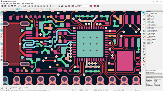
Design and manufacture real, useful printed circuit boards from scratch using KiCad 9. Each lesson produces one complete board for embedded systems, starting from a simple through-hole ATmega328P breakout and progressing to multi-layer STM32 and ESP32 boards with USB-C, WiFi, battery management, and motor control. Every board includes minimal firmware to verify it works. #KiCad #PCBDesign #EmbeddedSystems
Free and Open Source
KiCad is completely free with no feature limits, board size restrictions, or layer caps. Your designs are yours, stored in open formats, with no vendor lock-in.
Industry Capable
Interactive router with differential pair support, 3D board viewer, design rule checking, and direct export to every major fab house format. Used by CERN, Arduino, and thousands of professional projects.
Huge Component Library
Ships with thousands of symbols and footprints covering common ICs, connectors, and passives. Community libraries add tens of thousands more. Custom parts are straightforward to create.
Active Development
KiCad 9 brings an improved router, better DRC, enhanced 3D viewer, and smoother workflows. Regular releases backed by a growing developer community and corporate sponsors.
Each lesson follows a consistent cycle:
The Board What we are building, why it is useful, and the design choices behind it.
Schematic Capture Component selection, wiring, power distribution, ERC. Full walkthrough in KiCad 9.
PCB Layout Component placement strategy, routing, copper pours, design rules, DRC.
Manufacturing Output Gerbers, drill files, BOM, and the manufacturing method for that lesson (etching, CNC milling, or fab house).
Build and Test Soldering guidance, first power-on checklist, and minimal firmware to confirm the board works.
Lesson 1: ATmega328P Breakout Board
ATmega328P Through-Hole Breakout. Build a minimal Arduino-compatible board with ISP header, power LED, and pin headers. Learn KiCad 9 from scratch: project setup, schematic capture, PCB layout, and home etching. First firmware: blink an LED via ISP.
Lesson 2: ATmega328P Sensor Shield
ATmega328P Sensor Shield with SMD. Upgrade to SMD with an ATmega328P TQFP-32 board carrying I2C temperature/humidity and SPI light sensors. Introduction to SMD footprints, double-sided layout, and CNC milling for PCB fabrication.
Lesson 3: STM32 USB Development Board
STM32 USB Development Board. Design a Blue Pill style board with STM32F103, USB, crystal oscillator, SWD debug header, and 3.3V regulation. First professional fab house order: generate Gerbers, BOM, and pick-and-place files for JLCPCB.
Lesson 4: STM32 USB-C Four-Layer Board
STM32 USB-C Four-Layer PCB. Step up to a Black Pill style STM32F411 board with USB-C, LDO power regulation, and a 4-layer stackup. Learn power/ground plane design, via stitching, and impedance-aware routing.
Lesson 5: ESP32 WiFi/Bluetooth DevKit
ESP32 WiFi Bluetooth DevKit. Integrate an ESP32-WROOM module with USB-UART bridge, antenna keepout zone, auto-reset circuit, and impedance-matched RF trace. Layout considerations for wireless performance.
Lesson 6: ESP32 Battery IoT Sensor Node
ESP32 Battery IoT Sensor Node. Design a battery-powered ESP32-C3 board with TP4056 charge IC, solar input, BME280 environmental sensor, and deep sleep circuitry. Power-aware layout for long battery life.
Lesson 7: RP2040 USB-C Development Board
RP2040 USB-C Development Board. Build a board around the RP2040 with external flash, native USB-C, PIO headers, and RGB LED. QFN soldering considerations, high-speed routing, and 4-layer design.
Lesson 8: Motor Driver & Sensor Integration
Motor Driver Sensor Integration Board. Combine a DRV8833 H-bridge motor driver, MPU6050 IMU, current sensing, and screw terminals on one board. Mixed power and signal routing, thermal management, and protection circuits.
Lesson 9: Code-Based PCB Design
Code-Based PCB Design with KiCad Scripting. Recreate Lesson 1’s board using Python and KiCad’s scripting API. Introduction to SKiDL for programmatic netlists, parametric footprints, and automated DRC. A bridge to the future of code-driven electronics design.
| Skill | Lessons 1-2 | Lessons 3-4 | Lessons 5-6 | Lessons 7-8 | Lesson 9 |
|---|---|---|---|---|---|
| Components | Through-hole, basic SMD | Fine-pitch SMD, USB | RF modules, battery ICs | QFN, motor drivers | Programmatic |
| Layers | 1-2 layer | 2-4 layer | 2 layer (RF-aware) | 4 layer | Any |
| Routing | Manual, wide traces | Differential pairs intro | Impedance matching | High-speed, power | Automated |
| Manufacturing | Home etching, CNC mill | Fab house (JLCPCB) | Fab house | Fab house | Scripted output |
| Firmware | AVR ISP blink | USB CDC serial | WiFi scan, deep sleep | USB-C, PID control | None |
You should be comfortable with:
Helpful but not required:
Install KiCad 9 from kicad.org KiCad runs on Linux, macOS, and Windows. The installer includes all libraries.
Start with Lesson 1, which walks through KiCad 9 setup and produces your first complete PCB.
Work through lessons sequentially. Each builds on skills and patterns from earlier lessons.
Build the boards. The course is designed around manufacturing. Etching Lesson 1 at home or ordering Lesson 3 from JLCPCB is part of the learning.
Flash the firmware. Each lesson includes minimal code to verify your board works.