You have configured a PWM channel by writing a duty value into a register, and a UART by setting a baud divisor, without ever seeing what was on the other side of those registers. This lesson is what was on the other side. Build them yourself and the datasheets stop being incantations. #verilog #fpga #peripherals
Learning Objectives
By the end of this lesson, you will be able to:
Build a PWM generator from a counter and a comparator, and control its duty cycle.
Implement a UART transmitter with correct framing and baud-rate division.
Implement a UART receiver that samples each bit near its centre.
Build an SPI master from a shift register, and explain the clock-edge convention.
Explain what an MCU peripheral register is actually configuring.
What We Are Building
Four peripherals, from scratch
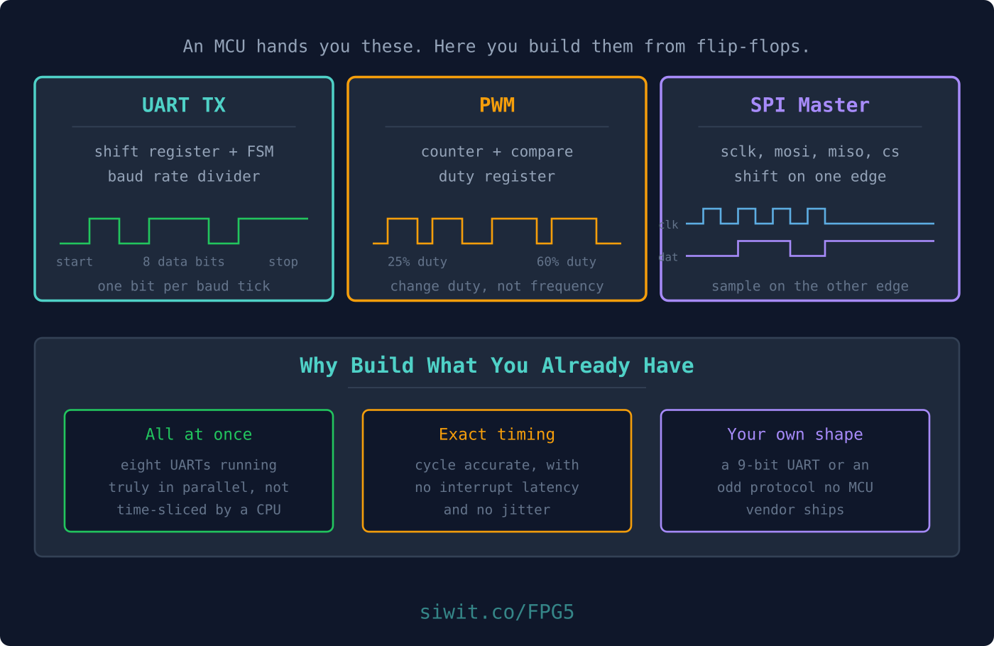
A PWM generator, a UART transmitter, a matching UART receiver, and an SPI master. Each is small enough to read in one sitting, and together they are most of what a microcontroller’s peripheral block does. Every one is verified in simulation before it goes near a board.
The pattern behind all four is worth naming up front, because once you see it the rest is detail:
A counter divides the system clock down to the rate the protocol needs.
A shift register turns a parallel value into a serial stream, or back again.
A small FSM sequences the framing around it.
That is it. Every serial peripheral you have ever configured is a variation on those three parts.
Counters as the Foundation: PWM
Pulse width modulation is the simplest of the four and the best illustration of the counter idea. Run a counter, compare it against a duty value, and drive the output high whenever the counter is below it.
pwm.v
module pwm #(
parameterinteger WIDTH =8
) (
inputwire clk,
inputwire rst,
inputwire [WIDTH-1:0] duty,
outputwire out
);
reg [WIDTH-1:0] cnt;
always @(posedge clk) begin
if (rst) cnt <=0;
else cnt <= cnt +1'b1;
end
assign out = (cnt < duty);
endmodule
That is the whole peripheral. Nine lines of logic, and it is the same nine lines inside every microcontroller you have used.
Some things worth reading off it:
The period is fixed by WIDTH, not by duty. An 8-bit counter wraps every 256 clocks, so at 27 MHz the PWM frequency is about 105 kHz regardless of duty. Changing duty changes only the ratio, which is exactly what you want for driving a motor or dimming an LED.
duty of 0 gives a permanently low output, because cnt < 0 is never true. duty at maximum gives 255 of 256 cycles high, not 256. Getting a true 100 percent needs one extra comparison, and most MCU peripherals have exactly the same off-by-one, which is why their datasheets talk about 255 rather than 256 steps.
duty can change at any time. There is no handshake. If it changes mid-period you get one slightly odd cycle, which for a motor is irrelevant. If it matters, register duty only at the wrap point.
Verified against both a quarter and a three-quarter duty:
Simulation output
PWM duty=64/256: high for 64 of 256 cycles PASS
PWM duty=192/256: high for 192 of 256 cycles PASS
Serial Out: The UART Transmitter
A UART frame is deliberately simple: the line idles high, drops low for one bit period to signal a start, sends eight data bits least significant first, then returns high for a stop bit. There is no clock line, which is why both ends must already agree on the bit rate.
One UART frame, 0xA5 = 10100101
idle start b0 b1 b2 b3 b4 b5 b6 b7 stop idle
___ ___ ___ ___ ___ _____
high | | | | | | | | | | | |
low | |________| |_| |____| |_| |_|
1 0 1 0 0 1 0 1
(sent LSB first, so this is 0xA5)
The baud divisor turns the system clock into bit periods. At 27 MHz and 115200 baud that is 27,000,000 / 115,200, or 234 clocks per bit.
The shift register line does the real work. shifter <= {1'b0, shifter[7:1]} moves every bit down one position and pads with a zero at the top, so each clock presents the next bit at shifter[0]. That single line is the whole of “serialise a byte”.
Note busy. Without it, a caller has no way to know when it is safe to send the next byte, and asserting start mid-frame would corrupt it. Every peripheral needs a way to say “not yet”, and this is the minimum version of it.
Serial In: The UART Receiver
Receiving is harder than transmitting, for one reason: you do not have the sender’s clock. You have to work out where each bit is from the shape of the signal alone.
The standard answer is to sample in the middle of each bit. Detect the falling edge that starts a frame, wait half a bit period, confirm the line is still low, and from then on sample every full bit period. Every sample now lands mid-bit, which gives the maximum tolerance to a clock mismatch between the two ends.
rx_0 <= rx; // the incoming line is asynchronous to us
rx_1 <= rx_0;
valid <=1'b0; // valid is a one-cycle pulse
case (state)
S_IDLE:
if (!rx_1) begin// falling edge: a start bit is beginning
tick <=0;
state <= S_START;
end
// Wait half a bit and confirm the start bit is still low. This both
// rejects noise and centres every later sample in its bit.
S_START:
if (tick >= (DIVISOR/2) -1) begin
if (!rx_1) begin
tick <=0;
bit_idx <=0;
state <= S_DATA;
endelse
state <= S_IDLE; // spurious edge, abandon the frame
endelse
tick <= tick + 1'b1;
S_DATA:
if (tick >= DIVISOR -1) begin
tick <=0;
shifter <= {rx_1, shifter[7:1]}; // LSB arrives first
if (bit_idx ==3'd7) state <= S_STOP;
else bit_idx <= bit_idx +1'b1;
endelse
tick <= tick + 1'b1;
S_STOP:
if (tick >= DIVISOR -1) begin
tick <=0;
state <= S_IDLE;
if (rx_1) begin// a valid frame ends high
data <= shifter;
valid <=1'b1;
end
endelse
tick <= tick + 1'b1;
default: state <= S_IDLE;
endcase
end
end
endmodule
Three details that separate this from a version that mostly works:
The two-flop synchroniser on rx. The incoming line belongs to somebody else’s clock domain. Sampling it directly can leave a flip-flop briefly undecided. Lesson 6 explains why properly; for now, note that every asynchronous input gets two flip-flops before anything looks at it.
Re-checking the start bit at the half-bit point. A single noise glitch on an idle line would otherwise start a frame and produce a garbage byte. Confirming the line is still low rejects most of that for free.
Checking the stop bit before asserting valid. If the line is not high when the stop bit is due, the framing was wrong, so the byte is discarded rather than reported. This is exactly what a real UART reports as a framing error.
Verifying both together
Wire the transmitter’s output straight into the receiver’s input and send several bytes, including the awkward all-zeros and all-ones cases:
Simulation output
RX got 0xa5 PASS
RX got 0x00 PASS
RX got 0xff PASS
bytes received = 3 of 3 PASS
Loopback is the right first test because it isolates your logic from any question about the other end’s baud rate.
SPI Master and Shift Registers
SPI is the honest one. It has a clock line, so both ends agree on timing by construction, and it is full duplex: every bit you send, you receive one back on the same edge.
Four wires: sclk (clock), mosi (master out, slave in), miso (master in, slave out), and cs_n (chip select, active low).
The convention that matters: the master changes mosi on one clock edge and both ends sample on the other. Getting this backwards is the classic SPI bug, and it produces data shifted by exactly one bit.
spi_master.v
module spi_master #(
parameterinteger HALF =4// system clocks per sclk half period
// Setup time: cs_n low and mosi valid before the first clock edge
S_LEAD: if (tock) state <= S_XFER;
S_XFER: if (tock) begin
if (!sclk) begin
sclk <=1'b1; // rising edge
shifter <= {shifter[6:0], miso}; // both ends sample here
endelsebegin
sclk <=1'b0; // falling edge
mosi <= shifter[7]; // present the next bit
end
edges <= edges +1'b1;
if (edges ==4'd15) state <= S_TRAIL;
end
S_TRAIL: if (tock) begin
sclk <=1'b0;
cs_n <=1'b1;
rx_data <= shifter;
busy <=1'b0;
state <= S_IDLE;
end
default: state <= S_IDLE;
endcase
end
end
endmodule
The elegance is in shifter <= {shifter[6:0], miso}. One shift register does both jobs: outgoing bits fall off the top into mosi, incoming bits enter at the bottom from miso. After sixteen edges the register holds exactly what the slave sent, and the slave holds what you sent. Full duplex for the price of one register.
S_LEAD and S_TRAIL exist because real slaves have setup and hold requirements around chip select. Dropping cs_n and clocking in the same cycle works in simulation and fails against about half of real parts.
Tested against a loopback slave model that returns a known byte:
Simulation output
SPI sent 0x5A, slave received 0x5a PASS
SPI master received 0x3c (slave sent 0x3C) PASS
cs_n released after transfer .......... PASS
What This Tells You About MCU Peripherals
Look back at what you just built and the register maps in a microcontroller datasheet stop being arbitrary:
What you wrote
What the datasheet calls it
DIVISOR parameter
The baud rate register, or a prescaler plus reload value
duty input
The PWM compare or capture register
busy output
The TXE or transmit-empty status flag
valid pulse
The RXNE or receive-not-empty flag, and its interrupt
Checking the stop bit
The framing error bit
HALF parameter
The SPI clock prescaler bits
S_LEAD and S_TRAIL
The chip-select setup and hold times in the timing diagram
And the reason an FPGA is worth this trouble: you can have as many as you like, all running at once. Eight UARTs on an MCU means either eight hardware blocks the vendor happened to provide, or bit-banging in software with the timing jitter that implies. Eight UARTs on an FPGA is a generate loop, and all eight run in genuine parallel with identical timing.
You can also build the peripheral nobody sells. A nine-bit UART, a protocol with an unusual frame, a PWM at a frequency no prescaler divides to. That freedom is the actual argument for the whole approach.
Application Questions and Solutions
Question 1: Garbled UART output
Characters sent from your FPGA UART arrive as garbage on the terminal, though the start and stop bits look present on the analyser. What is the first thing to check?
Click to reveal the solution
Check the baud rate. Garbled but framed data almost always means the transmit bit period does not match the receiver baud rate. ✅
Recompute the divider. The baud-rate counter divides the FPGA clock. Confirm the divisor matches the actual board clock frequency, not an assumed one. ✅
Verify bit order. UART sends the least significant bit first. A reversed shift direction produces consistent but wrong characters. ✅
Measure rather than assume. Put the analyser on one bit and time it. At 115200 baud a bit is 8.68 microseconds. If you measure 8.68, the timing is right and the fault is bit order or parity. If you measure something else, the divisor is wrong. ✅
Question 2: The SPI slave returns data shifted by one bit
An SPI master reads a sensor and every value comes back looking like the correct value shifted one bit left, with a zero in the least significant position. What is wrong?
Click to reveal the solution
Recognise the signature. A consistent one-bit shift is a clock-edge convention mismatch, not a wiring or logic fault. Random corruption would look different. ✅
Identify the two conventions. SPI has four modes, set by clock polarity and clock phase. They determine whether data is sampled on the rising or falling edge, and whether the clock idles high or low. ✅
Check what the slave expects. The sensor datasheet states its mode. If it samples on the falling edge and your master presents data on the falling edge, the slave captures the bit while it is still changing, and effectively reads the previous one. ✅
Fix it by moving your shift to the other edge, so the data is stable when the slave samples. In the module above, swap which branch of if (!sclk) does the shifting and which presents mosi. ✅
The wider lesson: with SPI, always find the mode in the datasheet before writing any code. Guessing has a one in four chance and debugging costs far more than reading.
Question 3: Why does the receiver wait half a bit?
A learner simplifies the UART receiver by sampling immediately on the falling edge and then every full bit period afterwards. It works perfectly in loopback and fails against a USB serial adapter. Explain.
Click to reveal the solution
Note what loopback hides. In loopback both ends share your clock exactly, so samples taken at bit boundaries land consistently and nothing drifts. The test proves the logic, not the timing margin. ✅
See what a real sender does. Its clock is close to yours but not identical. Over a ten-bit frame, a small percentage error accumulates into a large fraction of a bit period. ✅
Work out where the error lands. Sampling at a bit boundary means you are already at the worst possible place: any drift at all pushes the sample into the neighbouring bit. Sampling mid-bit leaves half a bit of margin in each direction. ✅
Quantify it. Mid-bit sampling tolerates roughly a 5 percent clock mismatch across a frame. Boundary sampling tolerates approximately none, which is why it passes loopback and fails everything else. ✅
Summary
Concept
Key Takeaway
The pattern
A counter for rate, a shift register for serialising, a small FSM for framing
PWM
A counter plus a compare value sets the duty cycle. The period comes from the counter width
UART framing
Idle high, start low, eight data bits least significant first, stop high
Baud divisor
System clock divided by baud rate. Compute it from the real clock, never an assumed one
Oversampling
The receiver waits half a bit, then samples every bit near its centre, for clock tolerance
Synchronise inputs
An asynchronous line gets two flip-flops before anything reads it
Framing errors
Check the stop bit before declaring a byte valid
SPI
One shift register does send and receive at once. Change data on one edge, sample on the other
Setup and hold
Real slaves need cs_n settled before the first clock edge
MCU link
These blocks are exactly what peripheral registers configure
You can now build the parts a microcontroller would have given you, and several at once. What you cannot yet do is store more than a handful of values, or safely hand data between two different clocks. Both are next.



Comments