The same Verilog that configures an FPGA can also become a custom chip. Until recently, seeing that process required an expensive licence and a non-disclosure agreement. Open tools changed that. In this capstone you take a design you already built and run it through the real steps a chip goes through on its way to a foundry, and you finish with a layout you can open and inspect. #asic #sky130 #librelane
Learning Objectives
By the end of this lesson, you will be able to:
Contrast an FPGA with an ASIC and explain when each makes sense.
Describe the ASIC flow: synthesis, floorplan, placement, clock tree, routing, and signoff.
Run LibreLane on the Sky130 PDK to take RTL to GDSII.
Open and interpret the resulting layout at a basic level.
State honestly what you have and have not achieved, and what getting silicon manufactured would actually involve.
What We Are Building
An earlier design taken to GDSII
You will take a small self-contained block, a counter, and push it through the open ASIC flow with the Sky130 process design kit to produce a GDSII layout, which is the file format a foundry uses to manufacture a chip. Then you will open it and look at what the tools built.
FPGA versus ASIC
Both run the same Verilog. What differs is what the Verilog becomes.
An FPGA is a chip that already exists, containing generic LUTs, flip-flops and routing, which your bitstream configures. An ASIC is a chip laid out for your design alone: the gates are the gates you need, placed where the tools chose to put them, connected by wires drawn for your netlist.
FPGA
ASIC
Up-front cost
The price of a board
Mask and engineering costs, large
Cost per unit at volume
Stays roughly the same
Much lower
Fix a bug
Reprogram in seconds
Redesign and re-manufacture
Speed and power
Good
Considerably better for the same logic
Time to first working part
Hours
Months
The decision is almost entirely about volume and risk. Non-recurring costs are what dominate, and they are the same whether you make one chip or a million, so they only amortise at scale. Below tens of thousands of units, an FPGA or even a cheap microcontroller usually wins on total cost, and it certainly wins on the ability to fix a mistake.
There is a third reason to run this flow that has nothing to do with shipping a chip: it teaches you what your Verilog costs. Nothing makes the price of a wide comparison or a deep adder chain concrete quite like watching a tool spend area and timing budget on it.
The ASIC Flow at a Glance
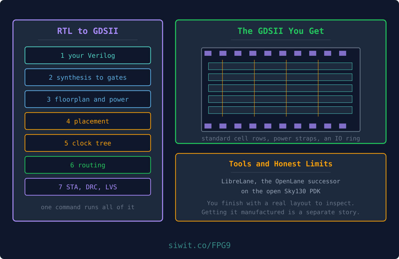
The journey from hardware description to physical layout runs through several automated stages. LibreLane drives all of them using a suite of open-source EDA tools.
1. RTL design and verification
The process begins with the register transfer level code you have been writing all course. This is also the last moment where fixing something is cheap, which is why Lesson 2 came so early.
2. Logic synthesis
The RTL is translated into a gate-level netlist. The synthesiser maps your behavioural code onto the actual physical logic gates, AND, OR, NOT, flip-flops, provided by a specific foundry’s process design kit (PDK), in our case the open SkyWater 130nm PDK.
This is the same Yosys you used for the FPGA, targeting a cell library instead of LUTs.
3. Floorplanning and power planning
Floorplanning determines the physical size of the chip core, creates the die boundary, and places any large macro blocks and the input and output pins.
Power planning creates the power distribution network, a grid of horizontal and vertical metal straps that ensures every cell gets adequate voltage without significant drop across the die.
4. Placement
The standard cells from the netlist are placed onto rows in the floorplan, in two phases. Global placement roughly positions connected cells near each other to minimise wire length. Detailed placement legalises those positions so cells align to the grid and do not overlap.
5. Clock tree synthesis
The clock must reach every flip-flop at very nearly the same moment, or timing analysis becomes meaningless. Clock tree synthesis builds a branching tree of buffers to distribute it evenly, minimising clock skew. On a real design this is often where most of the power goes.
6. Routing
Metal wires are drawn to connect the placed cells according to the netlist. Global routing plans general paths; detailed routing assigns actual metal layers and tracks, ensuring no shorts.
7. Signoff and verification
Three checks gate everything:
Static timing analysis (STA) confirms every path meets its timing constraints.
Design rule checking (DRC) confirms the layout obeys the foundry’s manufacturing rules, minimum wire width, spacing, and so on.
Layout versus schematic (LVS) confirms the physical layout matches the netlist it came from.
8. GDSII generation
The final output is a GDSII file, the industry-standard binary format describing the geometric shapes, text labels and layer information of the layout. This is what goes to the foundry.
Setting Up Sky130 and LibreLane
A note on names, because this changed recently
The flow most tutorials call OpenLane was developed at Efabless. Efabless closed at the end of February 2025, and the FOSSi Foundation released LibreLane in August 2025 as its successor: a ground-up reimplementation whose default “Classic” flow reproduces OpenLane closely and accepts the same configuration files.
So if you find a tutorial that says pip install openlane, it is not wrong so much as superseded. Use librelane, and expect your config.json to work unchanged. Command names and flags track the OpenLane 2 design closely, but check --help against the version you install rather than trusting any tutorial, including this one.
Prerequisites
You need Docker (or Podman) and a recent Python. The container carries every EDA tool and the PDK, which is what makes this reproducible rather than a two-day dependency hunt.
Fedora ships a very new Python. If the install below complains about the version, create a virtual environment on an older interpreter, for example python3.12 -m venv, and install there.
Install Docker and Python
brewinstall--caskdocker# then launch Docker Desktop once
brewinstallpython
Give Docker Desktop a generous memory allocation in its settings. The flow is happier with 8 GB or more.
Use WSL2 with the Ubuntu instructions, and install Docker Desktop with the WSL2 backend enabled. A native Windows install is not worth the trouble here.
Installing LibreLane
Use a virtual environment. It keeps this off your system Python and makes it trivial to discard.
Install LibreLane
python3-mvenv~/librelane-venv
source~/librelane-venv/bin/activate
pipinstall--upgradepip
pipinstalllibrelane
# Confirm it is there
python3-mlibrelane--version
Then pull the container and run the built-in smoke test, which verifies the whole toolchain end to end:
Pull the image and smoke test
python3-mlibrelane--dockerized--smoke-test
The first run downloads the image, which is several gigabytes and takes 5 to 10 minutes on a reasonable connection. The smoke test then builds a tiny design and reports success or failure. Do not continue until it passes, because every later error will be harder to interpret.
Running the Flow
The design
Keep the first run small. A counter is ideal: it has a clock, a reset, sequential logic and a bus output, which is enough to exercise every stage without taking an hour.
Create the design directory
mkdir-p~/asic_designs/counter_4bit
cd~/asic_designs/counter_4bit
counter_4bit.v
module counter_4bit (
inputwire clk,
inputwire rst,
inputwire enable,
outputreg [3:0] count
);
always @(posedge clk) begin
if (rst)
count <=4'b0000;
elseif (enable)
count <= count +1'b1;
end
endmodule
Note the synchronous reset. On an ASIC, a synchronous reset costs less area than an asynchronous one and avoids a whole category of timing problems on the reset path, so it is usually the right default here.
The configuration
config.json
{
"DESIGN_NAME": "counter_4bit",
"VERILOG_FILES": "dir::counter_4bit.v",
"CLOCK_PORT": "clk",
"CLOCK_PERIOD": 10.0,
"FP_SIZING": "absolute",
"DIE_AREA": "0 0 100 100",
"FP_CORE_UTIL": 40,
"PL_TARGET_DENSITY": 0.50
}
What each line does:
Key
Meaning
DESIGN_NAME
The top module. Must match the module name exactly
VERILOG_FILES
Sources. dir:: resolves relative to the config file
CLOCK_PORT
Which port is the clock. Without this, timing analysis has nothing to constrain
CLOCK_PERIOD
Target period in nanoseconds. 10.0 asks for 100 MHz
DIE_AREA
The die rectangle in microns. 100 by 100 is generous for a counter
FP_CORE_UTIL
Target percentage of the core filled with cells
PL_TARGET_DENSITY
How tightly placement packs cells. Lower leaves room for routing
Utilisation and density are the two you will actually tune. Pack too tightly and routing fails; pack too loosely and you waste area.
Run it
Run the flow
python3-mlibrelane--dockerized--run-tagfirst_run.
The flow synthesises, floorplans, places, builds the clock tree, routes, runs signoff, and writes a GDSII. Expect 5 to 10 minutes for a design this size. Results land under runs/first_run/, with the layout at:
Where the GDSII appears
runs/first_run/results/final/gds/counter_4bit.gds
Reading the Results
Producing a GDSII is not the achievement. Reading the numbers is.
The run summary
Look for three things, in this order:
Did signoff pass? A non-zero DRC or LVS count means the layout is not manufacturable, regardless of how good it looks.
Worst negative slack. Zero or positive means timing is met at your requested clock period. Negative means the design does not run that fast, and the number tells you by how much.
Area and cell count. For a 4-bit counter, expect a few dozen cells. If you see thousands, something in your RTL inferred far more logic than you intended, and that is worth chasing.
What you are looking at, roughly from the outside in: a ring of input and output pads around the edge, horizontal rows of standard cells filling the core, thick metal power straps crossing over them, and a dense mesh of thinner signal routing above that. Toggle layers on and off to see them separately, because everything at once is unreadable.
Find the four flip-flops holding count. They are the largest cells in the design, and seeing four of them is a satisfying confirmation that your always @(posedge clk) block became exactly what you expected.
Then try to break it
The most instructive thing you can do next is make the design worse and watch the numbers move:
Halve CLOCK_PERIOD and see whether slack goes negative.
Widen the counter to 32 bits and watch cell count and area climb.
Shrink DIE_AREA until routing fails, then read the error.
Each of those is a lesson about cost that no amount of reading delivers.
Routes to Real Silicon
Be clear about what you have: a layout you can inspect, produced by the same class of tools a foundry expects. What you do not have is a chip, and the path to one moved sharply in 2025.
As of this writing, mid-2026:
Efabless closed at the end of February 2025, and with it chipIgnite, which had been the standard affordable route onto Sky130 shuttles. Sky130 multi-project wafer runs were paused as a result.
ChipFoundry now runs a chipIgnite successor, on a thinner schedule than the old quarterly cadence.
Tiny Tapeout, the cheapest on-ramp for a very small design, was disrupted by the same closure and has been moving toward IHP’s open 130nm process and GlobalFoundries GF180.
wafer.space runs GF180MCU shuttles and publishes LibreLane project templates.
None of that diminishes the exercise. Sky130 remains the best documented open PDK, the flow runs identically whether or not a shuttle is currently taking submissions, and the understanding transfers to any process you later get access to.
Application Questions and Solutions
Question 1: FPGA prototype or straight to ASIC?
A team has a working design on an FPGA and expects to ship 5,000 units. A colleague argues they should tape out an ASIC immediately to cut unit cost. What is the flaw in that reasoning?
Click to reveal the solution
Weigh the non-recurring cost. An ASIC tape-out carries large one-time mask and engineering costs that only pay off at high volume. ✅
Compare against volume. Spread across 5,000 units, those one-time costs usually dwarf the per-unit saving, so an FPGA or a low-cost MCU is often cheaper overall at this scale. ✅
Consider risk and time. An FPGA can be reprogrammed after a bug, a manufactured ASIC cannot. At modest volumes the flexibility and lower risk of the FPGA typically win. ✅
Name the condition that would change the answer. Volume in the millions, or a hard requirement on power or speed that no available FPGA meets. Absent one of those, staying on the FPGA is the engineering decision, not the timid one. ✅
Question 2: The flow passes but the chip would not work
A design completes the flow with zero DRC violations and positive slack. It is still not ready to manufacture. Give two reasons, neither of which the flow would have caught.
Click to reveal the solution
The RTL might be wrong. The flow verifies that the layout matches the netlist and that the netlist meets timing. It never asks whether the netlist does what you wanted. Only your Lesson 2 testbenches answer that, which is why functional verification happens before any of this. ✅
The constraints might be wrong. Timing is met against CLOCK_PERIOD as declared. Declare 10 ns and run the part at 5 ns and the analysis was meaningless. The same applies to any input or output timing you did not constrain at all. ✅
A third, for credit: no reset strategy across the whole chip. A block that works in isolation can still come up in a bad state when integrated, if reset does not reach everything in a defined order. ✅
A fourth: nothing has been checked at temperature or voltage extremes. A single-corner run says the design works under one set of assumptions. Real signoff runs multiple corners. ✅
The general point: passing signoff means the layout faithfully implements the netlist. It says nothing about whether the netlist was worth implementing.
Question 3: Interpreting a bad area result
A learner pushes an 8-bit design through the flow and finds the cell count is roughly forty times what they expected. Where would you look first?
Click to reveal the solution
Suspect inferred storage. An array indexed by a computed value, or a case without a default, can infer latches or a large multiplexer where you intended simple logic. Check the synthesis log for latch and multiplexer warnings. ✅
Check arithmetic width. A counter declared 32 bits wide where 8 would do costs four times the flip-flops and a much wider carry chain. Size every register to what it actually holds. ✅
Read the synthesis report, not the layout. Cell counts per module are listed there, so you can see which block is responsible rather than guessing from the picture. ✅
Re-simulate after fixing. Reducing area by accidentally changing behaviour is not an improvement, so the Lesson 2 testbench runs again before the flow does. ✅
Summary
Concept
Key Takeaway
FPGA versus ASIC
Configurable fabric versus custom silicon, decided largely by volume and risk
PDK
The foundry’s cell library and rules. Sky130 is the open one



Comments