Having built a CPU, you now know something uncomfortable: the processor you spent a lesson on is worse than the one you can buy for two dollars. That is not a failure, it is the point. An FPGA earns its place doing what a microcontroller cannot, and the skill worth having is knowing where that line falls. #fpga #mcu #codesign
Learning Objectives
By the end of this lesson, you will be able to:
Compare FPGAs, microcontrollers and DSPs against the properties that actually decide a design.
Explain what a soft core and a system-on-chip are, and when either is worth it.
Partition a real system between an FPGA and an MCU, with reasoning you can defend.
Build a register interface between the two over SPI.
Recognise when an FPGA is the wrong answer, and say so.
What We Are Building
An SPI register interface, and the reasoning behind the split
A worked partition of a motor-control system, then the FPGA side of an SPI slave that exposes a small bank of registers, so a microcontroller can configure the hardware and read results back. Plus the honest test for whether you needed an FPGA in the first place.
FPGA versus MCU versus DSP
The three are not competitors so much as answers to different questions. What separates them is how they spend time.
FPGA
MCU
DSP
Concurrency
Genuine. Every block runs every cycle
One thing at a time, plus interrupts
One thing at a time, but very wide per step
Timing determinism
Cycle exact
Good, until an interrupt lands
Good
Best at
Many parallel channels, custom protocols, nanosecond timing
Decisions, sequencing, connectivity, anything with a library
You need many channels at once with identical timing. Eight quadrature encoders, sixteen PWM outputs, a hundred parallel comparisons.
The timing is hard real time in nanoseconds, not microseconds. Interrupt latency would be a large fraction of your budget.
The interface does not exist as a peripheral. An unusual protocol, a camera bus, a legacy parallel interface no vendor supports.
The data rate is high and the processing is simple. Filtering a stream as it arrives, where a CPU would be swamped just fetching it.
The logic is sequential and decision-heavy. State that depends on history, configuration, error handling.
You need connectivity and libraries. TCP, TLS, JSON, a filesystem, USB. All of it exists, tested, for free.
Cost and power dominate. A microcontroller costs a fraction of an FPGA and draws far less.
The requirements will change after shipping. Firmware updates are routine; a bitstream change is a bigger event.
This is the default. Reach for an FPGA when you can name the specific thing an MCU cannot do.
You have regular, heavy arithmetic on streaming data. Long FIR filters, FFTs, audio or vibration analysis.
The maths is well-trodden enough that mature libraries exist and you would rather use them than build blocks.
You want more throughput than an MCU without the development cost of an FPGA.
Note that the boundary is blurry now. Modern MCUs have DSP instructions, and FPGAs have hard multiply-accumulate blocks, so the choice often collapses into one of the other two.
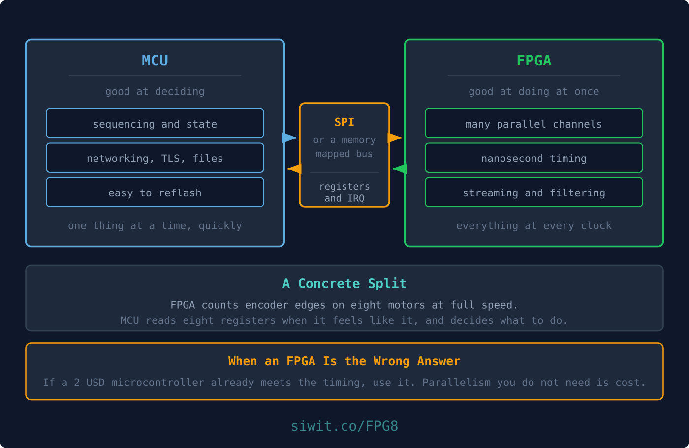
The heuristic engineers actually use, stated plainly: start with a microcontroller, and move a function to an FPGA only when you can name the specific requirement the MCU misses. Parallelism you do not need is cost, power and development time you paid for nothing.
System-on-Chip and Soft Cores
There is a third option between “FPGA” and “FPGA plus MCU”: put the processor inside the FPGA.
A soft core is a CPU described in Verilog and synthesised into the fabric, exactly like the mini CPU you built last lesson, only competently. Real ones are readily available: PicoRV32, VexRiscv and Neorv32 are all RISC-V cores that fit comfortably on a mid-range FPGA and run a real toolchain, meaning you can compile C for them with standard GCC.
A system-on-chip is that core plus memory plus peripherals plus your custom logic, all on one device, communicating over an internal bus.
Soft core inside the FPGA
Separate MCU alongside
Chip count
One
Two
Interface between them
An internal bus, no wires
SPI or a parallel bus, and its timing
CPU performance
Modest. Tens of MHz, no cache
Hundreds of MHz, real cache, FPU
Cost of the CPU
Fabric you could have used for logic
A few dollars of separate silicon
Software ecosystem
Bare metal or a small RTOS
Full vendor SDKs, networking stacks
Best when
The logic dominates and the software is simple
The software is substantial
The honest summary: a soft core is excellent when you need a little sequencing next to a lot of custom logic, and a poor deal when you need serious software. A 2 USD microcontroller outperforms most soft cores by a wide margin and comes with a networking stack. This lesson builds the two-chip version, because that is what most real designs look like.
Partitioning a System
Take a concrete example: closed-loop control of four brushless motors, with a web interface for monitoring and tuning.
Write down every function, then ask of each one what it actually demands.
Function
Demand
Where
Why
Read 4 quadrature encoders
4 channels, edges up to 1 MHz each
FPGA
Four counters running genuinely in parallel. An MCU would be interrupt-saturated
Generate 12 PWM outputs, 6-step commutation
12 channels, exact phase, dead-time
FPGA
Dead-time errors destroy transistors. Cycle-exact timing is not optional
Over-current trip
React within 1 microsecond
FPGA
Must not wait on software. Combinational comparison plus latch
PID loop, 1 kHz per motor
Modest maths, 4 instances
Either
See below
Read setpoints from a web request
TCP, TLS, JSON
MCU
The libraries exist. Building this in Verilog would be perverse
Log to an SD card
Filesystem
MCU
Same reason
Tuning, calibration, error recovery
Complex, changeable logic
MCU
Will be rewritten many times. Firmware updates are cheap
Two observations about how that table was filled in.
The trip is on the FPGA for a reason that is not performance. Over-current protection must work even if the software has crashed. Putting a safety interlock behind a scheduler is a design error regardless of how fast the scheduler is.
The PID loop could go either way, and that is the interesting one. At 1 kHz an MCU has a millisecond per iteration, which is an eternity. Put it on the MCU: it is easier to write, easier to tune, and trivially changeable. Move it to the FPGA only if you later need 50 kHz, or if jitter from other MCU activity starts showing up in the control response.
The principle underneath: put a function on the FPGA when it needs parallelism, hard timing, or independence from software. Put it on the MCU otherwise. Then resist moving anything else.
This mirrors the reasoning in local versus cloud control: the fast loop stays as close to the hardware as it must be, and the layer above earns its place by doing what the layer below cannot.
Building the FPGA-to-MCU Link
The two chips need to talk. The pattern that works, and that almost every real peripheral uses, is a register interface: the FPGA exposes a small bank of addressable registers, and the MCU reads and writes them.
That is worth pausing on. It is exactly what you have been doing to microcontroller peripherals all along, from the other side. Now you are the peripheral.
The protocol
Keep it as simple as possible. Two bytes per transaction:
A minimal register protocol over SPI
Byte 1:  [7]    read/write flag, 1 = write         [6:0]  register address
Byte 2:  data in (on a write) or data out (on a read)
cs_n frames the transaction. Deassert between transactions.
The FPGA side
Lesson 5 built an SPI master. Here you need the other end, an SPI slave, because the microcontroller drives the clock.
spi_reg_slave.v
module spi_reg_slave (
inputwire sclk,
inputwire cs_n,
inputwire mosi,
outputwire miso,
// register file exposed to the rest of the FPGA design
inputwire [7:0] status, // read-only, driven by your logic
inputwire [7:0] result, // read-only
outputreg [7:0] control, // written by the MCU
outputreg [7:0] setpoint // written by the MCU
);
reg [4:0] bit_cnt;
reg [7:0] shift_in;
reg [7:0] shift_out;
reg [7:0] cmd;
wire is_write = cmd[7];
wire [6:0] addr = cmd[6:0];
assign miso = shift_out[7];
// Read the addressed register into the outgoing shifter
always @(*) begin
case (addr)
7'd0: shift_out_next = status;
7'd1: shift_out_next = result;
7'd2: shift_out_next = control;
7'd3: shift_out_next = setpoint;
default: shift_out_next =8'h00;
endcase
end
reg [7:0] shift_out_next;
always @(posedge sclk orposedge cs_n) begin
if (cs_n) begin
bit_cnt <=0;
endelsebegin
shift_in <= {shift_in[6:0], mosi};
bit_cnt <= bit_cnt +1'b1;
if (bit_cnt ==5'd7) begin
cmd <= {shift_in[6:0], mosi}; // first byte complete
shift_out <= shift_out_next; // present the read value
end
if (bit_cnt ==5'd15) begin// second byte complete
if (is_write) begin
case (addr)
7'd2: control <= {shift_in[6:0], mosi};
7'd3: setpoint <= {shift_in[6:0], mosi};
default: ; // reads and unknown addresses do nothing
endcase
end
end
end
end
endmodule
Two things to note honestly about this block.
It is clocked by sclk, which belongs to the MCU. That makes the whole module a foreign clock domain inside your design. Anything in your FPGA logic that reads control or setpoint must treat them as crossing a domain boundary, using the discipline from the previous lesson: synchronise single-bit flags, and for multi-byte values either use a Gray-coded handshake or only sample them when a synchronised “updated” flag says they are stable. Getting this wrong is the classic integration bug, and it is intermittent, so it will pass your bench test.
Read-only and writable registers are deliberately separated.status and result are inputs to this module, driven by your logic. control and setpoint are outputs, driven by the MCU. Mixing the two directions in one register is how you get a value that neither side believes it wrote.
The MCU side
On the microcontroller it is ordinary SPI code. This is the pattern for any of the boards covered in the STM32 or ESP32 courses:
Register access from the MCU
#defineREG_STATUS0x00
#defineREG_RESULT0x01
#defineREG_CONTROL0x02
#defineREG_SETPOINT0x03
uint8_tfpga_read(uint8_taddr) {
uint8_ttx[2] = { addr &0x7F, 0x00 }; // top bit clear = read
uint8_trx[2];
spi_select();
spi_transfer(tx, rx, 2);
spi_deselect();
returnrx[1]; // data arrives in the second byte
}
voidfpga_write(uint8_taddr, uint8_tvalue) {
uint8_ttx[2] = { addr |0x80, value }; // top bit set = write
spi_select();
spi_transfer(tx, NULL, 2);
spi_deselect();
}
Start every integration by reading a register whose value you know. Put a fixed identifying constant at address 0 and read it first. If it comes back right, your wiring, clock polarity, bit order and framing are all correct, and every later problem is protocol rather than physical. If it comes back wrong, you have learned that before writing anything that could move a motor.
When an FPGA Is the Wrong Answer
This section exists because the failure mode of a course like this one is enthusiasm.
An FPGA is the wrong choice when:
A microcontroller already meets the requirement. If a 2 USD part hits your timing with margin, using an FPGA costs more money, more power, more board area and considerably more of your time, in exchange for nothing.
The requirements are still moving. Firmware iterates in seconds. A bitstream change is a synthesis run, a timing check and a reflash.
Nobody on the team can maintain it. A design only you can modify is a liability, and this is a real constraint rather than a soft one.
The volume is high and the margin is thin. At scale the unit cost difference dominates everything else. This is the same non-recurring versus per-unit argument that decides FPGA against ASIC, one step down the ladder.
The problem is really about software. Networking, file formats, user interfaces, protocols with libraries. Verilog is a bad language for all of it.
The corresponding test for when it is right: can you name the specific requirement a microcontroller misses, and is that requirement real rather than anticipated? “We might need more channels later” is not a requirement. “We need sixteen encoder channels at 1 MHz today” is.
Application Questions and Solutions
Question 1: Should this go on the FPGA or the MCU?
A design needs to timestamp incoming pulses to within 10 nanoseconds and also format the results into JSON for a web request. How would you partition it?
Click to reveal the solution
Separate the two needs. Nanosecond timestamping is hard real-time and parallel. JSON formatting and networking are flexible, sequential, library-heavy tasks. ✅
Put timing on the FPGA. Capture and timestamp the pulses in hardware, where the timing is deterministic and independent of any software load. ✅
Put formatting on the MCU. Hand the timestamps to the microcontroller over SPI, and let it build the JSON and handle the network, where a rich software stack already exists. ✅
Size the buffer between them. The FPGA captures at hardware rates and the MCU reads when it can, so a FIFO absorbs the mismatch. If the MCU falls behind, decide deliberately whether to drop oldest, drop newest, or assert back-pressure, and expose an overflow counter so the choice is visible. ✅
Question 2: The MCU reads a setpoint the FPGA never wrote
An MCU writes a 16-bit setpoint as two consecutive single-byte register writes. The FPGA logic occasionally acts on a value that is neither the old setpoint nor the new one. Explain, and fix it.
Click to reveal the solution
Notice the value is split. Two bytes are written in two separate SPI transactions, so between them the register pair holds the new low byte and the old high byte. Any logic sampling in that window sees a value that never existed. ✅
See that this is not a clock-domain problem. Synchronisers would not help. The corruption is at the protocol level: the update is not atomic. ✅
Add a commit mechanism. Have the MCU write both bytes into shadow registers, then write a separate apply bit. The FPGA copies shadow to live in one clock when it sees apply, so the transition is atomic. ✅
Then handle the clock domain as well. The apply bit is a single bit crossing from the SPI domain into your logic, so synchronise it with two flip-flops and act on its rising edge, exactly as in the debouncer from Lesson 4. ✅
The general pattern: multi-byte configuration needs a shadow-and-commit protocol. This is why real peripherals have “update” or “latch” bits that always seemed like clutter.
Question 3: Talk your colleague out of an FPGA
A colleague proposes an FPGA for a datalogger that samples four thermocouples once per second, timestamps the readings, and uploads them over WiFi. They argue it is more professional. Respond.
Click to reveal the solution
Test the timing requirement. One sample per second, on four channels. A microcontroller has hundreds of millions of cycles between samples. There is no timing pressure of any kind. ✅
Test the parallelism requirement. Four channels at 1 Hz is four reads per second, which any MCU does sequentially without noticing. Genuine parallelism buys nothing. ✅
Weigh what the FPGA costs here. WiFi means a TCP and TLS stack, which on an FPGA means adding a soft core and porting a network stack to it. On an ESP32 it is a library call. The FPGA route is more expensive, higher power, and much slower to build. ✅
Answer plainly. An ESP32 is the right tool: it samples, timestamps, and uploads with existing libraries, for a couple of dollars. The professional choice is the one that meets the requirement with the least complexity, not the one with the most impressive silicon. ✅
Summary
Concept
Key Takeaway
The default
Start with an MCU. Move a function to an FPGA only when you can name what the MCU misses
FPGA strengths
Real parallelism, nanosecond determinism, custom interfaces, independence from software
MCU strengths
Decisions, connectivity, libraries, cost, power, and cheap changes after shipping
Soft cores
PicoRV32, VexRiscv, Neorv32. Good for a little sequencing beside a lot of logic
Safety functions
Put interlocks in hardware. They must work when the software does not
Register interface
The FPGA becomes a peripheral. Exactly what you have been configuring all along
The SPI domain
An MCU-driven sclk is a foreign clock domain inside your design. Synchronise accordingly
Atomic updates
Multi-byte configuration needs shadow registers plus a commit bit
Start with a known value
Read a fixed constant register first to prove wiring, polarity and framing
Wrong tool
If a 2 USD MCU meets the requirement, an FPGA costs money, power and time for nothing
You can now build digital hardware, verify it, run it on a board, make peripherals, cross clock domains, execute a program, and place a function on the right side of a system boundary. One thing remains: taking a design past configurable silicon and into a chip of its own.


Comments