A microcontroller runs your instructions one after another, however fast the clock. Verilog does something else entirely: it describes hardware, and hardware does everything at the same time. That single difference is what trips up almost every programmer who comes to it, and it is what this lesson exists to fix. #verilog #hdl #digitaldesign
Learning Objectives
By the end of this lesson, you will be able to:
Write a Verilog module with input and output ports, and explain what it becomes in gates.
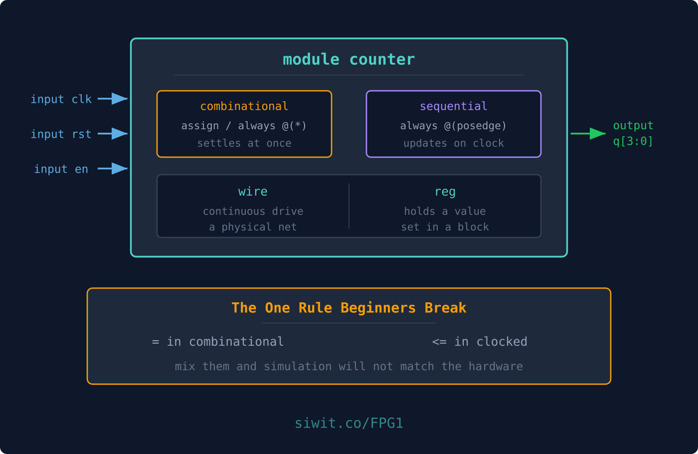
Distinguish combinational logic from sequential logic and choose wire versus reg correctly.
Describe the same circuit three ways, structurally, in dataflow, and behaviourally, and say when each is appropriate.
Apply the blocking (=) versus non-blocking (<=) rule and explain the bug it prevents.
Compose small modules into a larger design using hierarchy.
Simulate a design with Icarus Verilog and confirm it against a truth table.
What We Are Building
Logic gates, a 4-bit adder, and a counter
You will recreate the AND, OR, NOT, and XOR gates you built physically in Digital Electronics, this time as Verilog modules. Then you will compose them into a 4-bit ripple-carry adder, write a counter that advances on a clock edge, and simulate all of it without touching a board.
Tools used in this lesson:
Tool
Purpose
Icarus Verilog (iverilog)
Compile and simulate Verilog
GTKWave
View simulation waveforms
A text editor
VS Code with a Verilog extension is fine, so is anything else
No hardware is needed. You will not need an FPGA board until Lesson 4.
# Easiest route: install both from the iverilog Windows bundle
winget install --id IcarusVerilog.IcarusVerilog
# Or use WSL2 and follow the Ubuntu instructions above,
# which is the smoother path if you plan to reach Lesson 9.
Check that both work before going further:
Verify the install
iverilog-V
gtkwave--version
Why a Hardware Description Language
A program is a list of steps. A circuit is a shape. An HDL exists because you need a text file that describes a shape, not a sequence, and because that description has to be precise enough for a tool to turn into real gates.
Verilog does three jobs at once:
It documents the design in a form another engineer can read.
It simulates, so you can prove the design behaves correctly before committing it to anything physical.
It synthesises, meaning a tool reads it and produces an actual arrangement of gates and flip-flops.
That third job is the one with teeth. Anything you write has to be something hardware can physically be, and a good deal of legal Verilog is not synthesisable at all. Simulation will happily run a delay like #50, but no gate on earth implements “wait fifty nanoseconds.”
The level you will write at is called RTL, or register transfer level. The name is literal: you describe what combinational logic sits between the registers, and what moves from one register to the next on each clock edge. Get comfortable thinking in those terms and the rest of the course follows.
Verilog was created by Gateway Design Automation in the 1980s, became an IEEE standard, and remains one of the two dominant HDLs alongside VHDL. This course uses Verilog throughout.
From Schematic to Source: The Module
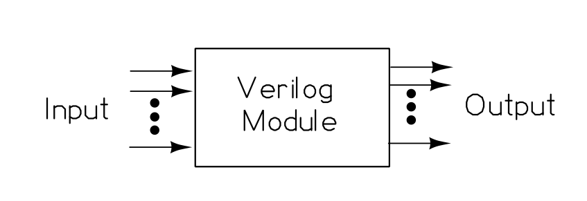
Everything in Verilog lives inside a module. A module has input ports, output ports, and logic in between. It is the unit of reuse, the same way a chip on a breadboard is: you wire up its pins and you do not care what is inside until you need to.
Figure: a module is a block with declared ports and internal logic
Here is the smallest useful one, a single AND gate:
and_gate.v
module and_gate (
inputwire a,
inputwire b,
outputwire y
);
assign y = a & b;
endmodule
Read it as a wiring instruction, not an instruction to execute. It says: there is a block called and_gate, it has two input pins and one output pin, and the output pin is permanently driven by the AND of the two inputs. There is no “when” about it. Change a and y follows, as fast as the gate can manage.
Module Syntax
General form
module<module_name> (<port_list>);
// Port definitions
// Description of the digital system
statement 1;
statement 2;
...
endmodule
Rules Worth Remembering
Rule
Description
1
The module name must be unique and must not clash with a Verilog keyword
2
Ports are how the module connects to the outside world
3
Port directions are declared inside the module
4
Every module closes with endmodule
5
Comments use // for one line, /* */ for several
Ports can be declared in the header, as in and_gate above, or listed and then declared separately. Both are common, and you will meet both in real code:
first_system.v, ports declared separately
module first_system (out1, out2, in1, in2);
// Port definitions
input in1, in2;
output out1, out2;
// Description of the digital system
and gate_and (out1, in1, in2);
orgate_or (out2, in1, in2);
endmodule
Wires versus Registers
Verilog gives you two ways to hold a value, and the names are actively misleading. Learn them once, properly, and a whole class of confusion disappears.
Type
What it means
Where you assign it
wire
A connection that is continuously driven by something else
assign statements, or a module’s output port
reg
A variable that keeps its value until something changes it
Inside always or initial blocks
The trap: reg does not mean “this becomes a hardware register.” It is a simulation storage type, nothing more. A reg assigned inside always @(*) synthesises to plain combinational logic with no flip-flop anywhere. A reg assigned inside always @(posedge clk) does become a flip-flop. The clock decides, not the keyword.
The practical rule is simply mechanical:
Driving something with assign? Declare it wire.
Driving something inside an always block? Declare it reg.
Get it wrong and the compiler tells you immediately, so this is a cheap mistake rather than an expensive one.
Three Ways to Describe the Same Hardware
Verilog offers three modelling styles. They are not three different circuits, they are three ways of writing down the same one, and mixing them inside a single module is normal practice.
Structural Modelling
You name the gates and wire them together yourself. Verilog has gate primitives built in, so and, or, xor and not are keywords you can instantiate directly. This is also called gate-level modelling.
Note that the output comes first in the port list of a gate primitive.
first_system.v, structural
module first_system (out1, out2, in1, in2);
// Port Definitions
input in1, in2;
output out1, out2;
// Internal Signals
wire and_out, or_out;
// Structural Modeling
and gate_and (and_out, in1, in2);
orgate_or (or_out, in1, in2);
xorgate_xor (out1, and_out, or_out);
notgate_not (out2, in2);
endmodule
This style is closest to a schematic, which makes it good for learning and tedious for anything large. Nobody builds a CPU this way.
Dataflow Modelling
You write the output as a function of the inputs and let the tool choose the gates. The keyword is assign, and the operators are the ones you would expect: & for AND, | for OR, ~ for NOT, ^ for XOR.
Syntax
assignoutput= function_of_inputs;
first_system.v, dataflow
module first_system (out1, out2, in1, in2);
// Port Definitions
input in1, in2;
output out1, out2;
// Internal Signals
wire and_out, or_out;
// Dataflow Modeling
assign and_out = in1 & in2;
assign or_out = in1 | in2;
assign out1 = and_out ^ or_out;
assign out2 =~in2;
endmodule
Both versions above produce identical hardware. Here is what they compute:
in1
in2
and_out
or_out
out1 (XOR)
out2 (NOT)
0
0
0
0
0
1
0
1
0
1
1
0
1
0
0
1
1
1
1
1
1
1
0
0
Dataflow is where most real combinational logic gets written. It is concise and it says what you mean.
Behavioural Modelling
You describe what the circuit does, inside a procedural block, and let the tool work out the structure. The keyword is always, followed by a sensitivity list saying what should retrigger it. More than one statement needs begin and end.
Syntax
always @ (sensitivity_list)
begin
statement 1;
statement 2;
...
end
first_system.v, behavioural
module first_system (out1, out2, in1, in2);
// Port Definitions
input in1, in2;
output out1, out2;
// Internal Signals
reg out1, out2;
// Behavioral Modeling
always @ (in1, in2) begin
out1 = (in1 & in2) ^ (in1 | in2);
out2 =~in2;
end
endmodule
Notice out1 and out2 are now reg, because they are assigned inside an always block. The hardware is still pure combinational logic. No clock appears anywhere, so no flip-flop is created.
Writing always @ (in1, in2) means “re-evaluate whenever in1 or in2 changes.” Forgetting a signal from that list is a classic bug: simulation goes stale while the synthesised hardware does the right thing, so the two disagree. Modern practice avoids the whole problem by writing always @(*), which asks the tool to work out the list for you:
Prefer this for combinational blocks
always @(*) begin
out1 = (in1 & in2) ^ (in1 | in2);
out2 =~in2;
end
Use always @(*) for combinational logic from here on.
Combinational Logic in Practice: a 4-Bit Adder
Time to build something with a carry chain. A full adder takes two bits and a carry in, and produces a sum bit and a carry out:
full_adder.v
module full_adder (
inputwire a,
inputwire b,
inputwire cin,
outputwire sum,
outputwire cout
);
assign sum = a ^ b ^ cin;
assign cout = (a & b) | (cin & (a ^ b));
endmodule
Chain four of them and the carry ripples from one stage to the next, exactly as it does when you add on paper:
Two things to notice. First, [3:0] declares a four-bit bus, and a[0] picks one bit out of it. Second, the instantiations use named port connection (.a(a[0])) rather than relying on position. Named connections are longer to type and save you from a whole category of silent wiring mistakes. Use them.
You could also have written the entire adder as assign {cout, sum} = a + b + cin; and the tool would build you something better optimised. The point of doing it the long way once is that you now know what + actually costs: four gate delays stacked end to end, which is exactly why wide ripple-carry adders are slow.
Sequential Logic: always @(posedge clk)
Everything so far settles on its own. Sequential logic is different: it remembers, and it changes only when the clock edge arrives. That is a flip-flop, and it is the other half of RTL.
counter_4bit.v
module counter_4bit (
inputwire clk,
inputwire reset,
outputreg [3:0] count
);
always @(posedge clk orposedge reset) begin
if (reset)
count <=4'b0000;
else
count <= count +1;
end
endmodule
Read the sensitivity list carefully. posedge clk means the block runs on the rising edge of the clock. Adding or posedge reset makes the reset asynchronous: it takes effect the moment it is asserted, without waiting for a clock edge.
count <= count + 1 is the line that makes this a counter. It says: whatever count is now, make it one greater at the next edge. Four flip-flops hold the value, and an adder sits between them computing the next one. That is the register transfer the name RTL refers to.
4'b0000 is a sized literal: four bits, binary, all zero. You will also see 4'd0 for decimal and 4'hF for hex. Get in the habit of sizing your literals, because unsized ones default to 32 bits and cause quiet truncation warnings.
Note also that count overflows silently from 4'b1111 back to 4'b0000. Four bits cannot hold sixteen, so it wraps. That is not a bug, it is arithmetic, but it is the kind of thing you have to decide about deliberately in hardware.
The Blocking versus Non-Blocking Rule
This is the single most common beginner bug in Verilog, and it is worth learning as a rule before you understand the theory.
The rule: use = in combinational always blocks, use <= in clocked always blocks.
That is it. Follow it and you will avoid the problem entirely. Here is why it exists.
= is blocking: statements take effect immediately and in order, like lines in a normal program. <= is non-blocking: the right-hand sides are all evaluated first, then every left-hand side updates together at the end of the time step.
Consider a two-stage shift register, where a should move to b and b to c on each edge. Written correctly:
Correct: non-blocking in a clocked block
always @(posedge clk) begin
b <= a;
c <= b;
end
Both right-hand sides are sampled before anything updates, so c receives the oldb. Two flip-flops, data marching along one stage per clock. Exactly what hardware does.
Now the same thing with blocking assignments:
Wrong: blocking in a clocked block
always @(posedge clk) begin
b = a;
c = b;
end
The first line executes and b is already a. The second line then copies that new value into c. So a reaches c in a single clock, and your two-stage shift register has collapsed into one stage. The hardware the tool synthesises may not even match what the simulator showed you, which is the worst kind of bug: it disappears when you look for it in one place and reappears in the other.
Keep to the rule and the question never comes up.
Building Bigger: Hierarchical Modules
Real designs are modules inside modules. You saw this already with the adder, where adder4 instantiated four copies of full_adder. The same idea applies at every scale, right up to the mini CPU you will build in Lesson 7.
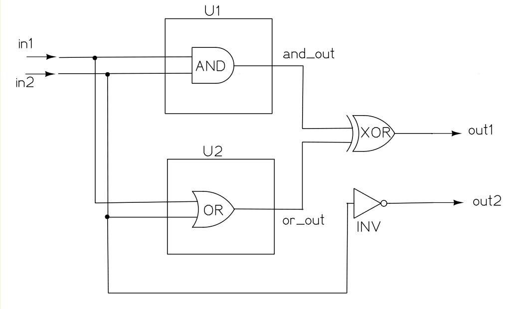
Figure: a top-level module built from two smaller ones
Split the AND and OR into their own modules:
and_module.v
module and_module (and_out, in1, in2);
    // Port Definitions    input  in1, in2;    output and_out;
    // Dataflow Modeling    assign and_out = in1 & in2;
endmodule
or_module.v
module or_module (or_out, in1, in2);
    // Port Definitions    input  in1, in2;    output or_out;
    // Dataflow Modeling    assign or_out = in1 | in2;
endmodule
Then wire them together in a parent, mixing structural instantiation with dataflow for the rest:
first_system.v, hierarchical
module first_system (out1, out2, in1, in2);
// Port Definitions
input in1, in2;
output out1, out2;
// Internal Signals
wire and_out, or_out;
// Structural Modeling: instantiate the submodules
and_module U1 (and_out, in1, in2);
or_moduleU2 (or_out, in1, in2);
// Dataflow Modeling for the rest
assign out1 = and_out ^ or_out;
assign out2 =~in2;
endmodule
U1 and U2 are instance names. Each instance is a separate physical copy of the logic. Instantiating and_module twice gives you two AND gates, not one shared between callers. This is the deepest difference from software: there is no such thing as calling the same function twice to save space. If you want two, you pay for two.
Running Your First Simulation
Icarus Verilog compiles your design, vvp runs it, and GTKWave shows you the result:
Compile, run, and view
# Compile the design and its testbench into a simulation binary
iverilog-ocounter_4bit_tb.vvpcounter_4bit_tb.v
# Run the simulation
vvpcounter_4bit_tb.vvp
# Open the waveform it produced
gtkwavecounter_4bit.vcd
You need a testbench to give the design inputs, since a module on its own has nothing driving its ports. Writing good testbenches is a skill in itself, and it is the whole subject of Lesson 2. For now, take it on trust that the three commands above are the loop you will run hundreds of times.
Application Questions and Solutions
Question 1: Build a 2-to-1 multiplexer
Write a Verilog module for a 2-to-1 multiplexer with inputs a, b, a select line sel, and output y, then describe how you would confirm it works.
Click to reveal the solution
Declare the module and ports. One output y, three inputs a, b, sel. ✅
Describe the logic. A multiplexer passes a when sel is 0 and b when sel is 1. The conditional operator expresses this directly. ✅
Choose the right type.y is driven by assign, so it is a wire. ✅
Confirm against the truth table in simulation for all four combinations of sel and the chosen input. ✅
mux2.v
module mux2 (
inputwire a,
inputwire b,
inputwire sel,
outputwire y
);
assign y = sel ? b : a;
endmodule
Question 2: Why does this counter never count?
A student writes the following and reports that count stays at zero in simulation. The reset is only asserted at the start. What is wrong, and what is the fix?
broken_counter.v
module broken_counter (
inputwire clk,
inputwire reset,
outputreg [3:0] count
);
always @(posedge clk) begin
if (reset)
count =4'b0000;
count = count +1;
count =4'b0000;
end
endmodule
Click to reveal the solution
Trace the block in order. Blocking assignments execute top to bottom within one clock edge, so the last line always wins. ✅
Identify the effect.count is incremented and then immediately overwritten with zero before the edge finishes, so the increment is never observable. ✅
Recognise the deeper problem. Assigning the same signal several times in one clocked block is a design smell. A flip-flop has one next-state value, so the code should compute one. ✅
Fix it by deciding the next value once, in an if / else, and using non-blocking assignment because this is a clocked block. ✅
fixed_counter.v
module fixed_counter (
inputwire clk,
inputwire reset,
outputreg [3:0] count
);
always @(posedge clk) begin
if (reset)
count <=4'b0000;
else
count <= count +1;
end
endmodule
Note this version has a synchronous reset, because reset is not in the sensitivity list and is only examined on a clock edge. That is usually the better choice on an FPGA, and Lesson 4 explains why.
Question 3: How many flip-flops does this create?
how_many.v
module how_many (
inputwire clk,
inputwire [3:0] a,
inputwire [3:0] b,
outputreg [3:0] x,
outputreg [3:0] y
);
always @(*) begin
x= a & b;
end
always @(posedge clk) begin
y <= a | b;
end
endmodule
Click to reveal the solution
Look at the first block. It is sensitive to *, not to a clock edge, so x is combinational despite being declared reg. Four AND gates, no storage. ✅
Look at the second block. It triggers on posedge clk, so y is registered. Four OR gates feeding four flip-flops. ✅
Count. Four flip-flops in total, all from the second block. ✅
The answer is four. This is the reg trap from earlier: the keyword tells you nothing about whether storage is created. Only the sensitivity list does.
Summary
Concept
Key Takeaway
Module
The reusable unit of hardware, with declared input and output ports
wire versus reg
wire for continuous drive, reg for values assigned in procedural blocks. reg does not imply a flip-flop
Modelling styles
Structural names the gates, dataflow writes a function, behavioural describes intent. All three synthesise
Combinational versus sequential
Combinational settles on its own, sequential updates on a clock edge
Blocking versus non-blocking
= in combinational blocks, <= in clocked blocks. This one rule prevents the most common Verilog bug
Hierarchy
Each instance is a separate physical copy. Two instances means twice the gates
RTL
Logic between registers, plus what moves on each edge. The level you design at
You can now describe hardware and you know what your description becomes. What you cannot yet do is prove it correct, and on hardware that matters far more than it does in software, because the feedback loop is so much slower. That is next.



Comments