A simulator is patient and forgiving. It will happily show you a design that no real chip could ever build, and it never once cares how long a signal takes to cross the die. Real hardware cares about both. This lesson is where your Verilog stops being a description and becomes a circuit. #fpga #verilog #hardware
Learning Objectives
By the end of this lesson, you will be able to:
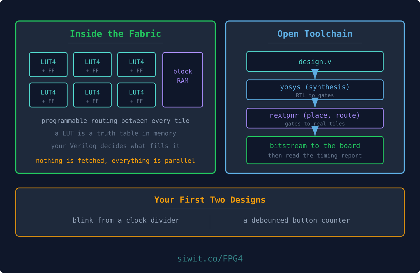
Describe what is inside an FPGA: lookup tables, flip-flops, block RAM, and routing.
Run the open toolchain to synthesise, place, route, and flash a design.
Map top-level signals to physical pins with a constraints file.
Read a basic timing report and understand what maximum clock frequency means.
Condition a real input, because physical buttons do not behave like simulated ones.
What We Are Building
Blink, then a debounced button counter
First a blinking LED, which proves the whole toolchain works end to end. Then a counter driven by a debounced push button, so you see a real input, sequential logic, and a real output all running together on hardware.
Choosing a board
Any FPGA with an open toolchain will do. Two are worth naming, and the course code runs on either.
Tang Nano 9K (recommended)
iCE40 boards (iCEstick, iCEBreaker)
Logic capacity
About 8,600 LUTs
1,280 on an iCEstick, 5,280 on an iCEBreaker
Cost
Roughly 15 to 20 USD
Roughly 30 to 70 USD
Extras on board
HDMI, LCD headers, 32 Mbit flash, 6 LEDs, buttons
LEDs, PMOD headers, some have no buttons
Open toolchain
Yosys, nextpnr, apicula, openFPGALoader
Yosys, nextpnr, IceStorm. The reference flow
Availability
Ships readily via Sipeed channels
Distributor stock, harder in some regions
The Tang Nano 9K is the primary recommendation, mostly because cost and availability decide whether
you can actually follow along, and because its extra capacity leaves room for the mini CPU later in
this course. The iCE40 flow is the older and better documented one, and if you already have a board
it is a perfectly good choice.
Everything else you need is a USB cable. Both boards have LEDs and the Tang Nano has buttons, so no
extra parts are required for this lesson.
What Is Inside an FPGA
A microcontroller has a fixed circuit that fetches your instructions and executes them one at a
time. An FPGA has no such circuit. It is a field of small configurable blocks, and your design
decides what each one becomes.
Lookup tables
The workhorse. A LUT is a tiny memory that implements a truth table. A 4-input LUT holds 16 bits,
one output value for each possible input combination. Configure those 16 bits and you have any
function of four inputs you like: an AND gate, a XOR, a majority vote, anything.
This is why an FPGA can be anything. It does not contain gates that get wired together. It contains
truth tables that get filled in.
Flip-flops
Next to almost every LUT sits a flip-flop. That is why the advice in the encoding section of the
previous lesson holds: flip-flops are effectively free, because they are there whether you use them
or not. Your always @(posedge clk) blocks land here.
Block RAM
Larger dedicated memories, a few kilobits each, arranged in columns. Far more efficient than
building storage out of flip-flops. When you write an array in Verilog and index it, the tool tries
to map it into block RAM, and Lesson 6 covers how to make sure it succeeds.
Routing
The most underappreciated part, and usually the majority of the silicon. A vast configurable
switching network connects any block to any other. Routing is also where most of your delay comes
from: on a large design, a signal spends more time travelling than computing.
The consequence
Nothing is fetched and nothing is sequential unless you made it so. A thousand LUTs all settle at
once, every clock cycle, whether you are using their results or not. Parallelism is not something
you opt into on an FPGA, it is the default, and serialising things is what costs you effort.
The Toolchain: From Verilog to Bitstream
Four stages, each a separate program:
Synthesis turns your Verilog into a netlist of the primitives this chip actually has. Yosys
does this.
Place and route decides which physical LUT each piece of logic lives in, and how the wires
run between them. nextpnr does this, and it is where timing is won or lost.
Bitstream packing turns the placed design into the binary the chip loads at power-up.
The oss-cad-suite bundle is by far the easiest route, since it ships Yosys, nextpnr, apicula and
openFPGALoader already built and matched to each other.
Add the source line to your shell profile to make it permanent. Also add yourself to the
plugdev group, or flashing will need root:
USB permissions
sudousermod-aGplugdev"$USER"
# then log out and back in
Install from apt
sudoaptupdate
sudoaptinstallyosysnextpnr-ice40fpga-icestorm
The packaged versions lag upstream. If synthesis rejects something it should accept, use the
oss-cad-suite bundle instead, following the Tang Nano tab.
Install on macOS
# Homebrew has the iCE40 flow
brewinstallyosysnextpnricestorm
# For Tang Nano, use the oss-cad-suite bundle for darwin
# from https://github.com/YosysHQ/oss-cad-suite-build/releases
Use WSL2 and follow the Ubuntu instructions. Native Windows builds of oss-cad-suite exist and
work, but USB passthrough for flashing is the part that causes trouble, and WSL2 with usbipd
is the better-trodden path.
Change --up5k --package sg48 to match your board. An iCEstick is --hx1k --package tq144.
Pin Constraints
Synthesis knows your design has a port called led. It has no idea which of the chip’s hundred-odd
pins that should be. A constraints file tells it, and getting it wrong is the single most common
reason a first design appears to do nothing.
Pin numbers are board-specific, not chip-specific. Copy them from your board’s own
documentation or schematic. A constraints file from a different board will build cleanly and do
nothing useful.
On-board LEDs are frequently active low. They light when you drive the pin to 0. If your blink
looks inverted, this is why, and it is not a bug in your counter.
Buttons need a pull resistor.PULL_MODE=UP gives you a pin that reads 1 when the button is
released and 0 when pressed. Which means a pressed button is a logic low, so remember to invert
it in your top level.
Your First Design: Blink
The board’s clock is far too fast to see. A 27 MHz clock toggling an LED directly would give you
13.5 million flashes a second, which looks exactly like a dimly lit LED. So divide it down:
blink.v
module blink #(
parameterinteger HALF_PERIOD =13_500_000// 27 MHz / 2 -> one toggle per half second
) (
inputwire clk,
inputwire rst,
outputreg led
);
reg [31:0] ticks;
always @(posedge clk) begin
if (rst) begin
ticks <=0;
led <=1'b0;
endelseif (ticks >= HALF_PERIOD -1) begin
ticks <=0;
led <=~led;
endelsebegin
ticks <= ticks +1;
end
end
endmodule
Note the reset, and note that it initialises led as well as ticks. Without it, led starts as
unknown in simulation, and ~unknown is still unknown, so the LED never toggles and the waveform is
a flat band of x forever. On real hardware the bitstream would have given you a defined starting
value and it would have worked, which is the worst kind of discrepancy: broken in simulation, fine on
the board, so you learn to distrust your simulator. Reset every sequential block and the question
never arises.
Conditioning a Real Input
Press a button and the metal contacts do not close once. They bounce, making and breaking contact
several times over a few milliseconds. Your simulated stimulus was a single clean edge. A real one is
a burst, and a counter that increments per edge will jump by five or six per press.
There is a second, subtler problem. The button is not synchronised to your clock, so it can change
at the exact instant a flip-flop samples it, leaving that flip-flop briefly undecided. Lesson 6
covers that properly; the fix here is the same two-flop synchroniser.
debouncer.v
module debouncer #(
parameterinteger STABLE_TICKS =270_000// about 10ms at 27 MHz
) (
inputwire clk,
inputwire rst,
inputwire noisy,
outputreg clean
);
reg sync_0, sync_1;
reg [31:0] count;
always @(posedge clk) begin
if (rst) begin
sync_0 <=0;
sync_1 <=0;
clean <=0;
count <=0;
endelsebegin
// Two-flop synchroniser: bring the asynchronous input into our clock domain
sync_0 <= noisy;
sync_1 <= sync_0;
// Only accept a change once it has held for STABLE_TICKS
if (sync_1 != clean) begin
if (count >= STABLE_TICKS -1) begin
clean <= sync_1;
count <=0;
endelse
count <= count + 1;
endelse
count <= 0;
end
end
endmodule
The logic is worth reading twice. The counter only runs while the synchronised input disagrees
with the current accepted value, and it resets the moment they agree again. So a bounce that flickers
back never accumulates enough consecutive ticks to be accepted. Only a change that genuinely holds
for the full window gets through.
Now count presses, on the rising edge of the clean signal rather than on its level:
press_counter.v
module press_counter #(
parameterinteger STABLE_TICKS =270_000
) (
inputwire clk,
inputwire rst,
inputwire btn,
outputreg [3:0] count
);
wire clean;
reg clean_d;
debouncer #(.STABLE_TICKS(STABLE_TICKS)) db (
.clk(clk), .rst(rst), .noisy(btn), .clean(clean)
);
always @(posedge clk) begin
if (rst) begin
count <=0;
clean_d <=0;
endelsebegin
clean_d <= clean;
if (clean &&!clean_d) // rising edge: exactly one press
count <= count +1;
end
end
endmodule
clean_d is the previous cycle’s value, so clean && !clean_d is true for exactly one clock cycle
per press. That one-cycle pulse from a level change is an idiom you will use constantly, and it is
worth recognising on sight.
Verify before you flash
Shrink the parameters and the whole thing simulates in milliseconds:
press_counter #(.STABLE_TICKS(4)) pc (.clk(clk), .rst(rst), .btn(btn), .count(count));
// ... then deliberately bounce the button six times before letting it settle
for (i =0; i <6; i = i +1) begin btn =~btn; #12; end
btn =1; #400;
btn =0; #400;
Simulation output
blink: 9 toggles in 40 cycles at HALF_PERIOD=4 PASS
count before press = 0
after ONE bouncy press: count=1 PASS
after a second press: count=2 PASS
Six input edges, one counted press. That is the debouncer earning its keep, and you know it works
before you have plugged anything in.
Timing and Maximum Frequency
Between any two flip-flops sits some combinational logic. On every clock edge, the first flip-flop
launches a value, that value has to travel through the logic and the routing, and it must arrive and
settle before the next edge. If it does not, the second flip-flop captures something meaningless.
The longest such path is the critical path, and its delay sets your maximum frequency. This is
the whole of timing in one idea.
nextpnr reports it:
Typical nextpnr output
Info: Max frequency for clock 'clk': 62.11 MHz (PASS at 27.00 MHz)
Info: Critical path report for clock 'clk' (posedge -> posedge):
Info: curr total
Info: 1.2 1.2 Source ticks_reg[0]_LUT4_Q
Info: 2.8 4.0 Net ticks[0] budget 37.0 ns (routing)
...
Two numbers matter. PASS at 27.00 MHz means the design meets the clock you asked for. 62.11
MHz is the headroom, and if it drops close to your target, the design is fragile: a small change
may push it over.
If you fail timing, the fix is almost never to try harder at place and route. It is to shorten the
critical path:
Add a register partway through a long chain of logic, so one deep path becomes two shallow
ones. This is called pipelining, and it costs one cycle of latency.
Simplify the arithmetic. The ripple-carry adder from Lesson 1 stacks four carry delays; a
wider one stacks more. Wide comparisons and long chains of if are the usual culprits.
Check you did not build a giant multiplexer by accident. A case over a wide signal, or
indexing a large array with a computed index, produces more logic than it looks like.
The unhelpful truth is that a design can pass timing and still fail on the board if you lied to the
tool about the clock. The constraints file declares the clock frequency, and if the real oscillator
is faster than you declared, the report is meaningless.
Application Questions and Solutions
Question 1: Works in simulation, wrong on the board
A counter behaves perfectly in simulation but on the FPGA it counts erratically when the button is
pressed. What is the most likely cause?
Click to reveal the solution
Suspect the input, not the logic. Simulation used clean, ideal stimulus. A real mechanical button bounces, producing many fast edges per press. ✅
Add a debouncer. Sample the button on the clock and require it to be stable for a set number of cycles before accepting a change. ✅
Synchronise it too. The button is asynchronous to your clock, so pass it through two flip-flops before using it, or a marginal sample can leave the first flip-flop briefly undecided. ✅
Confirm on hardware with a logic analyser on the raw and debounced signals to see the bounce removed. ✅
Question 2: The LED is lit but never blinks
A learner flashes the blink design onto a Tang Nano. The LED comes on and stays on. The design
simulates correctly. Give two plausible causes and how to distinguish them.
Click to reveal the solution
Cause one: the wrong pin. If led is constrained to a pin that is not connected to an LED, the LED you are watching is being driven by nothing, or by its default pull. Check the constraint against the board schematic. ✅
Cause two: the divider never rolls over. If HALF_PERIOD was left at a value far larger than intended, or the declared clock is much slower than the real one, the toggle happens so rarely it looks static. Compute the expected period and wait for it. ✅
Distinguish them cheaply. Set HALF_PERIOD to something tiny, rebuild, and watch with a scope or logic analyser. If the pin now toggles fast, the constraint is right and the divider value was the problem. If the pin never moves, the constraint is wrong. ✅
A third possibility worth ruling out: active-low LEDs. A design that is nominally driving 0 most of the time will look permanently lit. Invert and see. ✅
Question 3: Reading a failing timing report
A design targets 27 MHz. nextpnr reports a maximum frequency of 21 MHz, and the critical path runs
from a counter’s flip-flops, through a 32-bit comparison, to the next-state logic of an FSM. What are
two ways to fix it, and what does each cost?
Click to reveal the solution
Understand the path. A 32-bit comparison is a wide chain of logic. Feeding its result straight into next-state logic stacks both delays into a single clock period. ✅
Fix one: register the comparison. Compute expired into a flip-flop, and let the FSM use the registered version. The path is now split in two and each half is shallow. Cost: one cycle of latency, so a timer fires one tick late, which for a traffic light is irrelevant. ✅
Fix two: narrow the comparison. Counting to 13.5 million needs 24 bits, not 32. Sizing the counter to what it actually has to hold removes eight bits of comparison depth for free. Cost: none, beyond care in choosing the width. ✅
Choose. Narrowing costs nothing, so do it first. Register the result as well if you still miss timing. ✅
The general habit: when a path is too slow, look for the widest arithmetic or comparison in it before
you look anywhere else.
Summary
Concept
Key Takeaway
LUT
A tiny memory holding a truth table. This is why an FPGA can be any logic you like
Flip-flops
One beside almost every LUT, so they are effectively free
Block RAM
Dedicated memory columns, far cheaper than storage built from flip-flops
Routing
Most of the chip, and most of your delay on a large design
Toolchain
Synthesis, place and route, pack, flash. Yosys, nextpnr, then a board-specific packer
Constraints
Pin numbers are board-specific. A file from another board builds cleanly and does nothing
Active-low LEDs
Common on dev boards. An inverted-looking blink is usually this
Reset everything
Without a reset, led starts as x and ~x stays x. Broken in simulation, fine on hardware
Debouncing
Require an input to hold steady for a window before accepting a change
Edge detection
Compare a signal with its own delayed copy to get a one-cycle pulse
Timing
The longest flip-flop to flip-flop path sets maximum frequency. Fix it by shortening the path
You have a design running on real silicon, driven by a real input. Next you build the parts that a
microcontroller would otherwise have handed you.



Comments